The research of photodetectors is rooted in the principle of photoelectric effect, which has become indispensable in human society. Photodetectors convert light signals into electrical signals and represent a crucial subdivision within modern optoelectronic technology. They play significant roles in optical communications, remote sensing, biomedical applications, industrial automation, and more. Two-dimensional MoS2 has attracted considerable attention in optoelectronics due to its unique structure and performance characteristics. The research methods for photodetectors primarily include: Material Selection: Using semiconductor materials such as silicon, germanium, gallium arsenide, and indium arsenide. Silicon, in particular, is widely applied in optical communications, computer networks, medical diagnostics, and more. Technological Improvements: This involves high sensitivity detection techniques, automatic alignment technologies, and composite integration techniques to enhance the performance and application domains of photodetectors. Application Development: Exploring new applications of photodetectors in optical communications, medical imaging, security monitoring, etc., and improving their reliability and efficiency in practical applications.Research on photodetectors not only enhances their efficiency and performance in fields like communication, medicine, and security monitoring but also lays a solid foundation for future technological innovation and application expansion. With continuous advancements in technology, photodetectors are demonstrating vast application prospects and substantial market potential. Finally, the prospects and challenges associated with photodetectors in practical applications are also discussed.
| Published in | Engineering and Applied Sciences (Volume 9, Issue 4) |
| DOI | 10.11648/j.eas.20240904.11 |
| Page(s) | 53-62 |
| Creative Commons |
This is an Open Access article, distributed under the terms of the Creative Commons Attribution 4.0 International License (http://creativecommons.org/licenses/by/4.0/), which permits unrestricted use, distribution and reproduction in any medium or format, provided the original work is properly cited. |
| Copyright |
Copyright © The Author(s), 2024. Published by Science Publishing Group |
Two-Dimensional MoS2, Photodetectors, Photoelectric Performances
 (4)
(4) Materials | R (A W−1) | Response speed | D*(Jones) | Ref |
|---|---|---|---|---|
MoS2 | ~105-106 | – | 9.3×10¹² | [7 5] |
MoS2 | 880 | 4/9s | – | [27] |
MoS2 | 0.57 | 70/110μs | ~1010 | [5 1] |
MoS2/p-Si | 908.2 mA/W | 56/ 825 ns | 1.889×10¹³ | [4 6] |
MoS2 /n-Si | 11.9 | 30.5/71.6μs | 2.1×10¹⁰ | [ 48] |
MoS2/CdTe | 36.6 mA/W | 43.7/82.1μs | 6.1×10¹⁰ | [ 3] |
MoS2/CdSe | 2.5×10⁵ | 60/60ms | 1.24×10¹⁴ | [77] |
MoS2/GaAs | 35.2 mA /W | 3.4/15.6ms | 1.96×10¹³ | [5 0] |
MoS2/ZnO-QDs | 2267 | 12 /26s | 2.1×10¹¹ | [8 4] |
MoS2/Graphene | 104mA /W | 0.28/1.5s | – | [8 5] |
MoS2/PbS | 6×10⁵ | –/~0.35s | 5×10¹⁴ | [7 4] |
MoS2/GaAs | 0.419 | 17/31μs | 1.9 ×10¹⁴ | [ 77] |
MoS2/b-P | 22.3 | 15/70μs | 3.1×10¹¹ | [ 49] |
MoS2/b-AsP | 0.22 | 0.54/0.52 ms | 9.2 × 10⁹ | [ 86] |
MoS2/GaAs | 0.43mA /W | 1.87/3.53 ms | 2.28×10¹¹ | [ 87] |
MoS2/β-Ga2O3 | 2.05mA /W | – | 1.21×10¹¹ | [ 88] |
MoS2/MoTe2 | 0.86 | – | ~ 1011 | [ 89] |
MoS2/CuPc | ~1.98 | –/< 0.3 s | ~6.1×10¹⁰ | [21] |
Graphene/MoS2/Si | 0.6 | 17/48 ns, | 8×10¹² | [9 0] |
MoS2/WS2 | 2.3 | – | – | [9 1] |
MoS2/Si | ≈300mA/W | 3/40μs | ≈1013 | [9 2] |
DUV | Deep-Ultraviolet |
PDs | Photodetectors |
2D | Two-Dimensional |
TMDs | Transition Metal Dichalcogenides |
MoS2 | Molybdenum Disulphide |
NIR | Near-Infrared |
PV | Photovoltaic |
PTE | Photothermoelectric Effec |
| [1] | Liu Y, Yin J, Wang P, et al. High-Performance, Ultra-broadband, Ultraviolet to Terahertz Photodetectors based on Suspended Carbon Nanotube Films. Acs Appl Mater Interfaces. 2018; 10: 36304-36311. |
| [2] | Sang L, Liao M, Sumiya M. A Comprehensive Review of Semiconductor Ultraviolet Photodetectors: From Thin Film to One-Dimensional Nanostructures. Sensors. 2013; 13: 10482-10518. |
| [3] | Wang Y, Huang X, Wu D, et al. A room-temperature near-infrared photodetector based on a MoS2/CdTe p-n heterojunction with a broadband response up to 1700 nm. J Mater Chem C. 2018; 6: 4861-4865. |
| [4] | Ye L, Wang P, Luo W, et al. Highly polarization sensitive infrared photodetector based on black phosphorus-on-WSe2 photogate vertical heterostructure. Nano Energy. 2017; 37: 53-60. |
| [5] | Norton PR, Campbell III JB, Horn SB and Reago DA. Third-generation infrared imagers. Proc Spie 2000; 4130: 226-236. |
| [6] | Yao J, Zheng Z, Yang G. Layered-material WS2/topological insulator Bi2Te3 heterostructure photodetector with ultrahigh responsivity in the range from 370 to 1550 nm. J Mater Chem C. 2016; 4: 7831-7840. |
| [7] | Yao J, Zheng Z, Yang G. All-Layered 2D Optoelectronics: A High-Performance UV-vis-NIR Broadband SnSe Photodetector with Bi2Te3 Topological Insulator Electrodes. Adv Functional Mater. 2017; 27: 1701823. |
| [8] | Yao J, Shao J, Wang Y, et al. Ultra-broadband and high response of the Bi2Te3-si heterojunction and its application as a photodetector at room temperature in harsh working environments. Nanoscale. 2015; 7: 12535-12541. |
| [9] | Yin Z, Li H, Li H, et al. Single-Layer MoS2 Phototransistors. ACS Nano. 2012; 6: 74-80. |
| [10] | Mak KF, McGill KL, Park J, et al. The valley Hall effect in MoS2 transistors. Science. 2014; 344: 1489-1492. |
| [11] | Wu W, Wang L, Li Y, et al. Piezoelectricity of single atomic-layer MoS2 for energy conversion and piezotronics. Nature. 2014; 514: 470-474. |
| [12] | Rhyee J, Kwon J, Dak P, et al. High-mobility transistors based on largearea and highly crystalline CVD-grown MoSe2 films on insulating substrates. Adv Mater. 2016; 28: 2316-2321. |
| [13] | Zhang Y, Chang TR, Zhou B, et al. Direct observation of the transition from indirect to direct bandgap in atomically thin epitaxial MoSe2. Nat Nanotechnol. 2014; 9: 111-115. |
| [14] | Cheng R, Jiang S, Chen Y, et al. Few-layer molybdenum disulfide transistors and circuits for high-speed flexible electronics. Nat Commun. 2014; 5: 5143-5151. |
| [15] | Barja S, Wickenburg S, Liu Z, et al. Charge density wave order in 1D mirror twin boundaries of single-layer MoSe2. Nat Phys. 2016; 12: 751-756. |
| [16] | Splendiani A, Sun L, Zhang Y, et al. Emerging Photoluminescence in Monolayer MoS2. Nano Lett. 2010; 10: 1271-1275. |
| [17] | Wang H, Yu L, Lee Y-H, et al. Integrated Circuits Based on Bilayer MoS2 Transistors. Nano Lett. 2012; 12: 4674-4680. |
| [18] | Wi S, Kim H, Chen M, et al. Enhancement of Photovoltaic Reponse in Multilayer MoS2 Induced by Plasma Doping. ACS Nano. 2014; 8: 5270-5281. |
| [19] | Lee HS, Min S-W, Park MK, et al. MoS2 Nanosheets for Top-Gate Nonvolatile Memory Transistor Channel. Small 2012; 8: 3111-3115. |
| [20] | Kim S, Konar A, Hwang W-S, et al. High-mobility and low-power thin-film transistors based on multilayer MoS2 crystals Nat. Commun. 2012; 3: 1011-1017. |
| [21] | Pak J, Jang J, Cho K, et al. Enhancement of photodetection characteristics of MoS2 field effect transistors using surface treatment with copper phthalocyanine. Nanoscale. 2015; 7: 18780-18788. |
| [22] | Wang Q, Kalantar-Zadeh K, Kis A, et al. Electronics and opto-electronics of twodimensional transition metal dichalcogenides. Nat Nanotechnol. 2012; 7; 699-712. |
| [23] | Garciahernandez M, Coleman J. Corrigendum: materials science of graphene: a flagship perspective 2D Mater. 2016; 3: 019501. |
| [24] | Mak KF, Lee C, Hone J et al. Atomically Thin MoS2: A New Direct-Gap Semiconductor. Phys Rev Lett. 2010; 105: 136805-136808. |
| [25] | Radisavljevic B, Radenovic A, Brivio J, et al. Single-Layer MoS2 Transistors. Nat Nanotechnol. 2011; 6: 147-150. |
| [26] | Podzorov V, Gershenson M, Kloc C, et al. High-Mobility Field-Effect Transistors Based on Transition Metal Dichalcogenides. Appl Phys Lett. 2004; 84 3301-3303. |
| [27] | Lopez-Sanchez O, Lembke D, Kayci M, et al. Ultrasensitive photodetectors based on monolayer MoS2. Nat Nanotechnol. 2013; 8: 497-501. |
| [28] | Yoon Y, Ganapathi K, Salahuddin S. How Good Can Monolayer MoS2 Transistors Be. Nano Lett. 2011; 11; 3768-3773. |
| [29] | Ramakrishna Matte HSS, Gomathi A, Manna A K, et al. MoS2 and WS2 Analogues of Graphene. Angew Chem Int Ed. 2010; 49: 4059-4062. |
| [30] | Zeng Z, Yin Z, Huang X, et al. Single-Layer Semiconducting Nanosheets: High-Yield Preparation and Device Fabrication. Angew Chem Int Ed. 2011; 50: 11093-11097. |
| [31] | Eda G, Yamaguch H, Voiry D, et al. Photoluminescence from Chemically Exfoliated MoS2. Nano Lett. 2011; 11: 5111-5116. |
| [32] | Zhou K, Mao N, Wang H, et al. A Mixed-Solvent Strategy for Efficient Exfoliation of Inorganic Graphene Analogues. Angew Chem Int Ed. 2011; 50: 10839-10842. |
| [33] | Helveg S, Lauritsen JV, Lægsgaard E, et al. Atomic-Scale Structure of Single-Layer MoS2 Nanoclusters. Phys Rev Lett. 2000; 84: 951- 954. |
| [34] | Lauritsen J V, Kibsgaard J, Helveg S, et al. Size-dependent structure of MoS2 nanocrystals. Nat Nanotechnol. 2007; 2: 53-58. |
| [35] | Peng Y, Meng Z, Zhong C, et al. Hydrothermal Synthesis and Characterization of Single-Molecular-Layer MoS2 and MoSe2. Chem Lett. 2001; 8: 772-773. |
| [36] | Lee Y, Zhang X, Zhang W, et al. Synthesis of Large-Area MoS2 Atomic Layers with Chemical Vapor Deposition. Adv Mater. 2012; 24: 2320-2325. |
| [37] | Liu KK, Zhang W, Lee YH, et al. Growth of large-area and highly crystalline MoS2 thin layers on insulating substrates. Nano Lett. 2012; 12: 1538-1544. |
| [38] | Feng X, Tang Q, Zhou J, et al. Novel mixed-solvothermal synthesis of MoS2nanosheets with controllable morphologies. Cryst Res Technol. 2013; 48: 363-368. |
| [39] | Ji S, Yang Z, Zhang C, et al. Exfoliated MoS2 nanosheets as efficient catalysts for nelectrochemical hydrogen evolution. Electrochim Acta. 2013; 109: 269-275. |
| [40] | Lee S, Chu D, Song D, et al. Electrical and photovoltaic properties of residue-free MoS2 thin films by liquid exfoliation method. Nanotechnology. 2017; 28: 195703. |
| [41] | Ky DLC, Tran Khac BC, Le CT, et al. Friction characteristics of mechanically exfoliated and CVD-grown single-layer MoS2. Friction. 2017. |
| [42] | Li Y, Yin X, Wu W. Preparation of Few-Layer MoS2 Nanosheets via an Efficient Shearing Exfoliation Method. Ind Eng Chem Res. 2018; 57: 2838-2846. |
| [43] | Yu H, Zhu H, Dargusch M, et al. A reliable and highly efficient exfoliation method for water-dispersible MoS2 nanosheet. J Colloid Interface Sci. 2018; 514: 642-647. |
| [44] | Xu L, Gu Y, Li Y, et al. One-step preparation of molybdenum disulfide/graphene nano-catalysts through a simple co-exfoliation method for high-performance electrocatalytic hydrogen evolution reaction. J Colloid Interface Sci. 2019; 542: 355-362. |
| [45] | Dalila RN, Md Arshad MK, Gopinath SCB, et al. Current and future envision on developing biosensors aided by 2D molybdenum disulfide (MoS2) productions. Biosens Bioelectron. 2019; 132: 248-264. |
| [46] | Qiao S, Cong R, Liu J, et al. Vertical layered MoS2/Si heterojunction for ultrahigh and ultrafast photoresponse photodetector. J Mater Chem C. 2018; 6: 3233-3239. |
| [47] | Pak S, Jang AR, Lee J, et al. Surface functionalization-induced photoresponse characteristics of monolayer MoS2 for fast flexible photodetectors. Nanoscale. 2019. |
| [48] | Zhang Y, Yu Y, Mi L, et al. In Situ Fabrication of Vertical Multilayered MoS2/Si Homotype Heterojunction for High-Speed Visible-Near-Infrared Photodetectors. Small. 2016; 12: 1062-1071. |
| [49] | Ye L, Li H, Chen Z, et al. Near-Infrared Photodetector Based on MoS2/Black Phosphorus Heterojunction. ACS Photonics. 2016; 3: 692-699. |
| [50] | Jia C, Wu D, Wu E, et al. A self-powered high-performance photodetector based on a MoS2/GaAs heterojunction with high polarization sensitivity. J Mater Chem C. 2019; 7. |
| [51] | Tsai D, Liu K, Lien D, et al. Few-Layer MoS2 with High Broadband Photogain and Fast Optical Switching for Use in Harsh Environments. Acs nano. 2013; 7: 3905-3911. |
| [52] | Zhang C, Nakano K, Nakamura M, et al. Noncentrosymmetric Columnar Liquid Crystals with the Bulk Photovoltaic Effect for Organic Photodetectors. J Am Chem Soc. 2020; 142: 3326-3330. |
| [53] | Huang X, Mei C, Hu J, et al. Potential Superiority of p-Type Silicon-Based Metal-Oxide-Semiconductor Structures Over n-Type for Lateral Photovoltaic Effects. IEEE Electron Device Lett. 2016; 37: 1018-1021. |
| [54] | Qi J, Ma N, Yang Y, Photovoltaic-Pyroelectric Coupled Effect Induced Electricity for Self-Powered Photodetector System. Adv Mater Interfaces. 2017; 29: 1701189. |
| [55] | Li H, Li X, Park JH, et al. Restoring the Photovoltaic Effect in Graphene-based van der Waals Heterojunctions towards Self-Powered High-Detectivity Photodetectors. Nano Energy. 2019; 57: 214-221. |
| [56] | Mech RK, Mohta N, Chatterjee A, et al. High Responsivity and Photovoltaic Effect Based on Vertical Transport in Multilaye α-In2Se3. Phys Status Solidi A. 2020; 217: 1900932. |
| [57] | Buscema M, Island JO, Groenendijk DJ, et al. Photocurrent generation with two-dimensional van der Waals semiconductors. Chem Soc Rev. 2015; 44: 3691-3718. |
| [58] | Shaygan M, Davami K, Kheirabi N, et al. Single-crystalline CdTe nanowire field effect transistors as nanowire-based photodetector. Phys Chem Chem Phys. 2014; 16: 22687-22693. |
| [59] | Shinde SS, Rajpure KY. Fabrication and performance of N-doped ZnO UV photoconductive detector. J Alloys Compd. 2012; 522: 118-122. |
| [60] | Li J, Yan X, Sun F, et al. Anomalous photoconductive behavior of a single InAs nanowire photodetector. Appl Phys Lett. 2015; 107: 263103. |
| [61] | Su W, Weng W, Wang Y, et al. Mo1-x WxS2-based photodetector fabrication and photoconductive characteristics. Jpn J Appl Phys. 2017; 56: 032201. |
| [62] | Wang P, Liu Y, Yin J, et al. A tunable positive and negative photoconductive photodetector based on a gold/graphene/p-type silicon heterojunction. J Mater Chem C. 2019; 7: 887-896. |
| [63] | Yang Z, Jiang B, Zhang Z, et al. The photovoltaic and photoconductive photodetector based on GeSe/2D semiconductor van der Waals heterostructure. Appl Phys Lett. 2020; 116: 141101. |
| [64] | Saenz GA, Karapetrov G, Curtis J, et al. Ultra-high Photoresponsivity in Suspended Metal-Semiconductor-Metal Mesoscopic Multilayer MoS2 Broadband Detector from UV-to-IR with Low Schottky Barrier Contacts. Sci Rep. 2018; 8: 1276-1286. |
| [65] | Qin F, Gao F, Dai M, et al. Multilayer InSe-Te van der Waals heterostructures with ultrahigh rectification ratio and ultrasensitive photoresponse. ACS Appl Mater Interfaces. 2020; 12: 37313-37319. |
| [66] | Lu X, Jiang P, Bao X. Phonon-enhanced photothermoelectric effect in SrTiO3 ultra-broadband photodetector. Nat Commun. 2019; 10. |
| [67] | Gosciniak J, Rasras M, Khurgin J. Ultrafast Plasmonic graphene photodetector based on channel photo-thermoelectric effect. ACS Photonics. 2020; 7: 488-498. |
| [68] | He X, Wang X, Nanot S, et al. Photothermoelectric p-n Junction Photodetector with Intrinsic Broadband Polarimetry Based on Macroscopic Carbon Nanotube Films. Acs Nano. 2013; 7: 7271-7277. |
| [69] | Kallatt S, Umesh G, Bhat N, et al. Photoresponse of atomically thin MoS2 layers and their planar heterojunctions. Nanoscale. 2016; 8: 15213-15222. |
| [70] | Liu J, Zhou Y, Lin Y, et al. Anisotropic Photoresponse of the Ultrathin GeSe Nanoplates Grown by Rapid Physical Vapor Deposition. ACS Appl Mater Interfaces. 2019; 11: 4123-4130. |
| [71] | Sarwat SG, Youngblood N, Au YY, et al. Engineering Interface-Dependent Photoconductivity in Ge2Sb2Te5 Nanoscale Devices. ACS Appl Mater Interfaces. 2018; |
| [72] | Guo W, Dong Z, Xu Y, et al. Sensitive Terahertz Detection and Imaging Driven by the Photothermoelectric Effect in Ultrashort-Channel Black Phosphorus Devices. Adv Sci. 2020; 7: 1902699. |
| [73] | Ra H S, Kwak DH, Lee JS. A hybrid MoS2 nanosheet-CdSe nanocrystal phototransistor with a fast photoresponse. Nanoscale. 2016; 8: 17223-17230. |
| [74] | Kufer D, Nikitskiy I, Lasanta T, et al. Hybrid 2D-0D MoS2-PbS Quantum Dot Photodetectors. Adv Mater. 2015; 27: 176-180. |
| [75] | Yang Y, Huo N, Li J. Sensitized monolayer MoS2 phototransistors with ultrahigh responsivity. J Mater Chem C. 2017; 5: 11614-11619. |
| [76] | Long M, Wang P, Fang H, et al. Progress, Challenges, and Opportunities for 2D Material Based Photodetectors. Adv Funct Mater. 2018; 1803807. |
| [77] | Xu Z, Lin S, Li X, et al. Monolayer MoS2/GaAs heterostructure self-driven photodetector with extremely high detectivity. Nano Energy. 2016; 23: 89-96. |
| [78] | Li G, Li Z, Chen J, et al. Self-powered, high-speed Sb2Se3/Si heterojunction photodetector with close spaced sublimation processed Sb2 Se3 layer. J Alloys Compd. 2017; 737: 67-73. |
| [79] | Huang R, Zhang J, Wei F, et al. Ultrahigh responsivity of ternary Sb-Bi-Se nanowire photodetectors. Adv Funct Mater. 2014; 24: 3581-3586. |
| [80] | Kan H, Zheng W, Lin R, et al. Ultrafast Photovoltaic-Type Deep Ultraviolet Photodetectors Using Hybrid Zero-/Two-Dimensional Heterojunctions. ACS Appl Mater Interfaces. 2019; 11: 8412-8418. |
| [81] | Liu S, Li M, Su D, et al. Broad-Band High-Sensitivity ZnO Colloidal Quantum Dots/Self-Assembled Au Nanoantennas Heterostructures Photodetectors. ACS Appl Mater Interfaces. 2018; 10: 32516-32525. |
| [82] | Ma S, Li K, Xu H, et al. A Lattice-mismatched PbTe/ZnTe Heterostructure with High-speed Mid-infrared Photoresponses. ACS Appl Mater Interfaces. 2019; |
| [83] | Li L, Lou Z, Chen H, et al. Stretchable SnO2-CdS interlaced-nanowire film ultraviolet photodetectors. Sci China Mater. 2019; |
| [84] | Nazir G, Khan MF, Akhtar I, et al. Enhanced photoresponse of ZnO quantum dot-decorated MoS2 thin films. RSC Adv. 2017; 7: 16890-16900. |
| [85] | Xu H, Wu J, Feng Q, et al. High responsivity and gate tunable graphene-MoS2 hybrid phototransistor. Small. 2014; 10: 2300-2306. |
| [86] | Long M, Gao A, Wang P, et al. Room temperature high-detectivity mid-infrared photodetectors based on black arsenic phosphorus. Sci Adv. 2017; 3: e1700589. |
| [87] | Zhang Y, Yu Y, Wang X, et al. Solution assembly MoS2 nanopetals/GaAs n–n homotype heterojunction with ultrafast and low noise photoresponse using graphene as carrier collector. J Mater Chem C. 2016; 5: 140-148. |
| [88] | Zhuo R, Wu D, Wang Y, et al. A self-powered solar-blind photodetector based on a MoS2/β-Ga2O3 heterojunction. J Mater Chem C. 2018; 6. |
| [89] | Ahn J, Kang JH, Kyhm JH et al. Self-Powered Visible-Invisible Multiband Detection and Imaging Achieved Using High-Performance 2D MoTe2/MoS2 Semivertical Heterojunction Photodiodes. ACS Appl Mater Interfaces. 2020; 12: 10858-10866. |
| [90] | Yu Y, Li Z, Lu Z, et al. Graphene/MoS2/Si Nanowires Schottky-NP Bipolar van der Waals Heterojunction for Ultrafast Photodetectors. IEEE Electron Device Lett. 2018; 39. |
| [91] | Xue Y, Zhang Y, Liu Y, et al. Scalable Production of a Few-Layer MoS2/WS2 Vertical Heterojunction Array and Its Application for Photodetectors. Acs Nano. 2016; 10: 573-580. |
| [92] | Wang L, Jie J, Shao Z, et al. MoS2/Si Heterojunction with Vertically Standing Layered Structure for Ultrafast, High-Detectivity, Self-Driven Visible-Near Infrared Photodetectors. Adv Funct Mater. 2015; 25: 2910-2919. |
APA Style
Sun, X., Jian, J., Jian, Z. (2024). Application of 2-D Molybdenum Disulfide in the Field of Photoelectric Detection. Engineering and Applied Sciences, 9(4), 53-62. https://doi.org/10.11648/j.eas.20240904.11
ACS Style
Sun, X.; Jian, J.; Jian, Z. Application of 2-D Molybdenum Disulfide in the Field of Photoelectric Detection. Eng. Appl. Sci. 2024, 9(4), 53-62. doi: 10.11648/j.eas.20240904.11
AMA Style
Sun X, Jian J, Jian Z. Application of 2-D Molybdenum Disulfide in the Field of Photoelectric Detection. Eng Appl Sci. 2024;9(4):53-62. doi: 10.11648/j.eas.20240904.11
@article{10.11648/j.eas.20240904.11,
  author = {Xiaochen Sun and Jiaying Jian and Zengyun Jian},
  title = {Application of 2-D Molybdenum Disulfide in the Field of Photoelectric Detection
},
  journal = {Engineering and Applied Sciences},
  volume = {9},
  number = {4},
  pages = {53-62},
  doi = {10.11648/j.eas.20240904.11},
  url = {https://doi.org/10.11648/j.eas.20240904.11},
  eprint = {https://article.sciencepublishinggroup.com/pdf/10.11648.j.eas.20240904.11},
  abstract = {The research of photodetectors is rooted in the principle of photoelectric effect, which has become indispensable in human society. Photodetectors convert light signals into electrical signals and represent a crucial subdivision within modern optoelectronic technology. They play significant roles in optical communications, remote sensing, biomedical applications, industrial automation, and more. Two-dimensional MoS2 has attracted considerable attention in optoelectronics due to its unique structure and performance characteristics. The research methods for photodetectors primarily include: Material Selection: Using semiconductor materials such as silicon, germanium, gallium arsenide, and indium arsenide. Silicon, in particular, is widely applied in optical communications, computer networks, medical diagnostics, and more. Technological Improvements: This involves high sensitivity detection techniques, automatic alignment technologies, and composite integration techniques to enhance the performance and application domains of photodetectors. Application Development: Exploring new applications of photodetectors in optical communications, medical imaging, security monitoring, etc., and improving their reliability and efficiency in practical applications.Research on photodetectors not only enhances their efficiency and performance in fields like communication, medicine, and security monitoring but also lays a solid foundation for future technological innovation and application expansion. With continuous advancements in technology, photodetectors are demonstrating vast application prospects and substantial market potential. Finally, the prospects and challenges associated with photodetectors in practical applications are also discussed.
},
 year = {2024}
}
TY  - JOUR
T1  - Application of 2-D Molybdenum Disulfide in the Field of Photoelectric Detection

AU  - Xiaochen Sun
AU  - Jiaying Jian
AU  - Zengyun Jian
Y1  - 2024/08/27
PY  - 2024
N1  - https://doi.org/10.11648/j.eas.20240904.11
DO  - 10.11648/j.eas.20240904.11
T2  - Engineering and Applied Sciences
JF  - Engineering and Applied Sciences
JO  - Engineering and Applied Sciences
SP  - 53
EP  - 62
PB  - Science Publishing Group
SN  - 2575-1468
UR  - https://doi.org/10.11648/j.eas.20240904.11
AB  - The research of photodetectors is rooted in the principle of photoelectric effect, which has become indispensable in human society. Photodetectors convert light signals into electrical signals and represent a crucial subdivision within modern optoelectronic technology. They play significant roles in optical communications, remote sensing, biomedical applications, industrial automation, and more. Two-dimensional MoS2 has attracted considerable attention in optoelectronics due to its unique structure and performance characteristics. The research methods for photodetectors primarily include: Material Selection: Using semiconductor materials such as silicon, germanium, gallium arsenide, and indium arsenide. Silicon, in particular, is widely applied in optical communications, computer networks, medical diagnostics, and more. Technological Improvements: This involves high sensitivity detection techniques, automatic alignment technologies, and composite integration techniques to enhance the performance and application domains of photodetectors. Application Development: Exploring new applications of photodetectors in optical communications, medical imaging, security monitoring, etc., and improving their reliability and efficiency in practical applications.Research on photodetectors not only enhances their efficiency and performance in fields like communication, medicine, and security monitoring but also lays a solid foundation for future technological innovation and application expansion. With continuous advancements in technology, photodetectors are demonstrating vast application prospects and substantial market potential. Finally, the prospects and challenges associated with photodetectors in practical applications are also discussed.

VL  - 9
IS  - 4
ER  -
School of Materials and Chemical Engineering, Xi’an Technological University, Xi’an, China
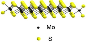
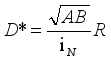
Figure 1. Molecular structure of MoS2 [21].
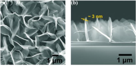
Figure 2. From the top to the bottom, and (b) Cross-sectional SEM images of V-MoS2. [46].
Figure 3. Optical image (a) and AFM topography image (b) of monolayer MoS2 [47].
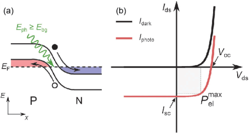
Figure 4. Schematic diagram of the photovoltaic effect. (a) Band alignment in a PN junction. (b) I-V curves in the dark and under illumination [57].
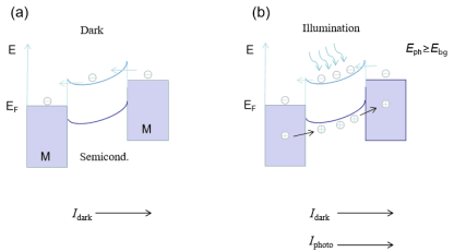
Figure 5. Schematic diagram of the photoconductive effect. (a) without illumination. (b) Under illumination [57].
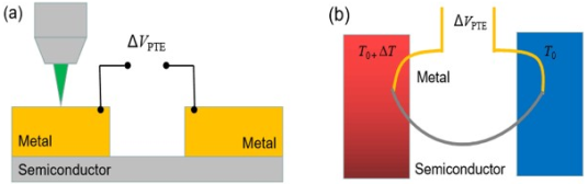
Figure 6. Schematic diagram of the photo-thermoelectric effect. (a) Schematic of a field-effect transistor. (b) Thermal circuit corresponding to the device depicted in (a) [57].
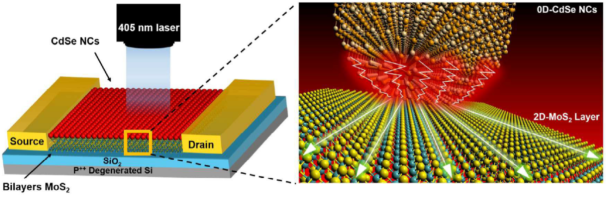
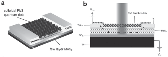
Figure 8. a 3D view and b Cross sectional view of MoS2/PbS quantum dot photodetector [74].
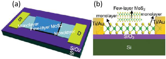
Figure 9. (a) Top view and (b) side view of the MoS2 phototransistor schematic diagram [75].
Figure 10. Schematic illustration of the V-MoS2/Si heterojunction PD [46].
Information