Research Article | | Peer-Reviewed

Comparative Performance Evaluation of Conventional and Tuned Single-Stage Common-Emitter Transistor Amplifiers Using Multisim 11.0

Received: 29 July 2026     Accepted: 10 August 2026     Published: 9 September 2026
Views:       Downloads:
Abstract

The frequency response of transistor amplifiers is a key performance characteristic that determines their suitability for broadband and frequency-selective applications. This study comparatively evaluates the performance of a conventional single-stage common-emitter transistor amplifier and a tuned single-stage common-emitter transistor amplifier using NI Multisim 11.0. Both amplifier configurations were designed and simulated under identical operating conditions using a 2N2222A NPN transistor, a 12 V supply, identical biasing networks, and the same passive components. The only design difference was the replacement of the collector resistor in the conventional amplifier with a parallel LC resonant circuit in the tuned amplifier. The frequency response of both amplifiers was evaluated over the frequency range of 10 Hz to 100 MHz, and the voltage gains were calculated from the simulated output waveforms and expressed in decibels (dB). The results showed that the conventional amplifier maintained a nearly constant mid-band gain of approximately 54 dB over a wide frequency range, demonstrating excellent broadband performance. In contrast, the tuned amplifier produced a maximum gain of approximately 72.04 dB at its designed resonant frequency of 1 kHz, but exhibited a much narrower bandwidth due to its frequency-selective characteristics. The comparative analysis confirms that the conventional amplifier is better suited for broadband signal amplification, whereas the tuned amplifier is more appropriate for narrow-band and radio-frequency applications requiring high gain at a specific frequency. These findings provide useful guidance for selecting suitable transistor amplifier configurations for broadband and frequency-selective electronic and communication applications.

Published in Journal of Electrical and Electronic Engineering (Volume 14, Issue 5)
DOI 10.11648/j.jeee.20261405.11
Page(s) 211-222
Creative Commons

This is an Open Access article, distributed under the terms of the Creative Commons Attribution 4.0 International License (http://creativecommons.org/licenses/by/4.0/), which permits unrestricted use, distribution and reproduction in any medium or format, provided the original work is properly cited.

Copyright

Copyright © The Author(s), 2026. Published by Science Publishing Group

Keywords

Common-emitter Transistor Amplifier, Tuned Amplifier, Frequency Response, Bandwidth, Resonant Frequency, Voltage Gain, Bode Magnitude Plot, Small-signal Amplifier

1. Introduction
Transistor amplifiers are among the most fundamental building blocks of analog electronic systems because they provide voltage, current, and power amplification required in communication, instrumentation, audio, and signal-processing applications. Among the various transistor amplifier configurations, the common-emitter (CE) transistor amplifier is the most widely used because it offers high voltage gain, moderate input impedance, and excellent overall performance in small-signal amplification . Depending on the intended application, common-emitter amplifiers may be designed either as conventional broadband amplifiers or as tuned amplifiers to achieve specific frequency response characteristics.
The conventional single-stage common-emitter transistor amplifier is designed to provide relatively uniform gain over a wide range of frequencies, making it suitable for broadband signal amplification in audio amplifiers, instrumentation systems, and general-purpose electronic circuits . In contrast, the single-stage tuned common-emitter transistor amplifier incorporates an LC resonant circuit in the collector network to provide maximum voltage gain at its resonant frequency while attenuating signals outside the desired frequency band. Consequently, tuned amplifiers are widely used in radio-frequency (RF) receivers, transmitters, intermediate-frequency (IF) stages, and communication systems where frequency selectivity is required ..
The frequency response of an amplifier is one of the most important parameters used to evaluate its performance because it determines the range of frequencies over which the amplifier can provide useful gain. This response is commonly represented using a Bode magnitude plot, which illustrates the variation of voltage gain with frequency on a logarithmic scale. Important performance parameters, including mid-band gain, lower cutoff frequency, upper cutoff frequency, bandwidth, and resonant frequency, can be determined directly from the amplifier's frequency response . Therefore, frequency response analysis provides an effective means of comparing different amplifier configurations under identical operating conditions.
Several researchers have investigated transistor amplifier performance using simulation and experimental approaches. . discussed the theoretical operation and frequency response characteristics of common-emitter transistor amplifiers, highlighting the influence of coupling capacitors, transistor parasitic capacitances, and bias conditions on amplifier bandwidth. presented a comprehensive analysis of transistor amplifier frequency response and demonstrated the effects of internal transistor capacitances on high-frequency performance. examined the design and operation of small-signal transistor amplifiers, emphasizing the relationship between gain, bandwidth, and transistor biasing. explained the operation of tuned amplifiers and showed how LC resonant circuits improve gain and frequency selectivity in communication applications. Similarly, demonstrated the usefulness of Multisim simulation software for analyzing electronic circuits and validating amplifier performance before hardware implementation. proposed an analytical approach for evaluating the exact frequency response of common- emitter amplifiers, demonstrating improved accuracy in determining gain and pole locations compared with conventional approximation methods. experimentally investigated the frequency response of a common-emitter BJT amplifier and demonstrated the influence of coupling, bypass, and Miller capacitances on amplifier bandwidth. developed a state-space modeling approach for bipolar junction transistor amplifiers and demonstrated the dynamic frequency-dependent behavior of common-emitter amplifier configurations. proposed recursive shunt-circuit transformations for transistor frequency-response analysis, providing a rigorous approach for evaluating gain, bandwidth, and stability in analog amplifier circuits. compared several single-stage amplifier configurations through simulation and showed that amplifier topology significantly influences voltage gain, impedance characteristics, and application suitability.
Although these studies provide comprehensive theoretical explanations of transistor amplifier operation, most focus on individual amplifier configurations rather than providing a direct comparison between a conventional single-stage common-emitter transistor amplifier and a single-stage tuned common-emitter transistor amplifier under identical operating conditions. Furthermore, relatively few studies employ Multisim 11.0 to compare the two amplifier configurations using identical transistor parameters, supply voltage, bias conditions, and input signal characteristics while evaluating their frequency response, bandwidth, and frequency-selective behaviors. This limitation makes it difficult to clearly demonstrate the practical differences between broadband and tuned amplifier performance.
This study addresses this gap by designing, simulating, and comparing a conventional single-stage common-emitter transistor amplifier and a single-stage tuned common-emitter transistor amplifier using Multisim 11.0 under identical operating conditions. The frequency response of both amplifiers is evaluated over the frequency range of 10 Hz to 100 MHz, this frequency range was selected to capture the low-frequency, mid-band, and high-frequency operating regions of both amplifier configurations, thereby enabling a comprehensive evaluation of their broadband and frequency-selective characteristics and the corresponding voltage gains are analyses using Bode magnitude plots. The comparison focuses on gain, bandwidth, resonant frequency, and frequency-selective characteristics in order to determine the advantages and limitations of each amplifier configuration. The findings are expected to provide useful guidance for students, researchers, and practicing engineers in selecting appropriate amplifier configurations for broadband and narrow-band electronic applications.
2. Methodology
This study adopted a simulation-based comparative research approach to evaluate the performance of a conventional single-stage common-emitter transistor amplifier and a single-stage tuned common-emitter transistor amplifier. A simulation-based approach was employed because it enables a controlled comparison of amplifier configurations while eliminating variations associated with component tolerances, measurement uncertainties, and environmental conditions that may arise in experimental hardware implementations. Both amplifier configurations were designed and simulated using NI Multisim 11.0, which provides reliable circuit simulation and frequency-domain analysis tools for evaluating analog electronic circuits under identical operating conditions. The circuits were designed using identical transistor parameters, supply voltage, biasing conditions, and passive component values to ensure that any observed differences in performance resulted solely from the collector load configuration. The conventional amplifier employed a resistive collector load, whereas the tuned amplifier utilized a parallel LC resonant circuit to achieve frequency-selective amplification . The research methodology comprised four sequential stages: (i) design of the conventional amplifier, (ii) design of the tuned amplifier, (iii) simulation and frequency-response analysis of both amplifier configurations, and (iv) comparative evaluation of their voltage gain, frequency response, bandwidth, resonant characteristics, phase response, and output waveform quality.
2.1. Circuit Design
The circuit design involved the development of two amplifier configurations: a conventional single-stage common-emitter transistor amplifier and a single-stage tuned common-emitter transistor amplifier, both employing a 2N2222A NPN bipolar junction transistor. Both amplifier configurations employed the same supply voltage, voltage-divider bias network, quiescent operating point, source resistance, collector and emitter resistors, and coupling and bypass capacitors to ensure a fair performance comparison . The only design difference between the two amplifier configurations was the collector load. The conventional amplifier employed a resistive collector load, whereas the tuned amplifier utilized a parallel LC resonant circuit to provide frequency-selective amplification .. The detailed design procedures, component calculations, and circuit implementations for both amplifier configurations are presented in the following sections.
(VCC)2.1.1. Selection of the Supply Voltage
The supply voltage was selected to ensure safe operation of the transistor by remaining well below its maximum collector-emitter voltage rating. According to the 2N2222A transistor datasheet, the maximum collector-emitter voltage (VCEO) is 40 V . Therefore, a supply voltage of 12 V was selected because it provides a safe operating margin below the transistor's maximum voltage rating while remaining suitable for laboratory implementation and practical amplifier design. The selected supply voltage also served as the basis for determining the transistor quiescent operating point and the subsequent biasing component values.
VCC=12V(1)
2.1.2. Selection of the Operating Point (Q-Point)
The operating point (Q-point) defines the steady-state DC operating conditions of the transistor and is specified by the collector current (IC), base current (IB), and collector-emitter voltage (VCE) . A properly selected Q-point ensures that the transistor operates in the active region throughout the input signal cycle, thereby minimizing distortion and enabling linear amplification. The base current was determined using Equation (2):
IB=ICβ(2)
To obtain a nearly symmetrical output voltage swing while maintaining transistor operation within the active region, the collector-emitter voltage was selected within the range
VCC3<VCE<VCC2(3)
For the selected supply voltage of VCC=12V, the lower limit of the recommended operating range is
VCE=VCC3=4V
A collector current of IC=4mA was selected as the design specification for the low-power small-signal amplifier. Assuming a transistor current gain of β=200, the corresponding base current is calculated as follows:
IB=4×10-3200=2×10⁻⁵A=20μA
Accordingly, the selected DC operating point for the amplifier design is
1) VCC=12V
2) IC=4mA
3) IB= 20μA
These operating conditions provide sufficient collector-emitter voltage for nearly symmetrical signal amplification while maintaining transistor operation in the active region.
2.1.3. Selection of the Collector and Emitter Resistors
The collector resistor (RC) and emitter resistor (RE) were selected to establish the desired DC operating point while ensuring stable transistor operation, adequate voltage gain, and improved thermal stability. For a common-emitter transistor amplifier operating in the active region, the emitter current is approximately equal to the collector current ., that is,
ICIE(4)
For symmetrical output voltage swing and improved thermal stability, the collector and emitter resistors were selected to have approximately equal value. Applying Kirchhoff's Voltage Law (KVL) to the collector-emitter loop gives
VCC=ICRC+VCE+IERE(5)
This follows directly from
1) ICIE
2) RCRE
VCC=IC(RC+RE)+VCE
Hence,RC=VCC - VCE2IC(6)
Substituting the selected design values, VCC=12V, VCE=4V and IC=4mA gives
RC=12-42×4×10-3=80.008=1000Ω=1
Since RERC,
For design symmetry and improved thermal stability, the emitter resistor was selected equal to the collector resistor; therefore,
RC=RE=1
These resistor values establish the desired quiescent operating point, provide appropriate voltage drops across the collector and emitter resistors, improve thermal stability, and maintain sufficient collector-emitter voltage for nearly symmetrical, low-distortion signal amplification. The same resistor values were adopted for the tuned amplifier to ensure identical operating conditions during the comparative performance evaluation.
(R1and R2)2.1.4. Selection of the Bias Resistors
The bias resistors R1 and R2 form a voltage-divider bias network that establishes the required base voltage and ensures stable transistor operation . A properly designed voltage-divider bias reduces the influence of transistor current gain (β) variations and improves thermal stability by maintaining a nearly constant base voltage . Applying Kirchhoff's Voltage Law (KVL) to the base-emitter loop gives
I2R2=VBE+VE(7)
where
1) I2 is the current flowing through R2,
2) VBE is the base-emitter voltage,
3) VE is the emitter voltage
The emitter voltage is obtained from, VE=REIE
Since IEIC=4mA and RE=1 then VE=4×10⁻³(1000)=4V
Assuming a silicon transistor, VBE=0.6V
Therefore, VB=VBE+VE=0.6+4=4.6V
Applying KVL to the voltage-divider network, VCC=I1R1+VB where I1=12+IB
Hence,
R1=VCC - VBI2+IB(8)
To minimize the effect of base current on the divider voltage, the divider current is selected to be much greater than the base current. A common design practice is
I210IB
In this study, I2=25IB was selected to provide improved bias stability.
Since IB=20μA, then I2=25×20μA=500μA=0.5mA
Because IBI2, the base current may be neglected. Equation (8) becomes
R1VCC-VBI2
Therefore, R1=12-4.60.5×10-3=7.40.0005=14.8
Similarly, R2=4.60.5×10-3=9.2
Thus, R1=14.8  and R2=9.2
These resistor values establish the required base bias voltage, maintain transistor operation within the active region, and improve operating-point stability against variations in transistor current gain and temperature.
(Rg)2.1.5. Selection of the Source Resistance
The source resistance (Rg) represents the internal resistance of the signal source supplying the input AC signal to the amplifier. The source resistance influences signal transfer from the source to the amplifier input and consequently affects the overall voltage gain and input signal amplitude . The voltage gain, which serves as one of the principal performance parameters evaluated in this study, is defined as the ratio of the output voltage to the input voltage:
AV=VoutVin(9)
where:
1) AV is the voltage gain,
2) Vout is the output voltage, and
3) Vin is the input voltage.
In this study, the source resistance was fixed at 5 Ω, corresponding to the internal output resistance of the NI Multisim function generator. This value was maintained throughout the simulations to ensure identical excitation conditions for both amplifier configurations. A sinusoidal input signal with a peak amplitude of 10 mV was applied to both amplifiers so that any observed performance differences resulted solely from the amplifier topology. Under ideal small-signal conditions, the voltage gain is approximately proportional to the ratio of the collector resistance to the source resistance, and may be expressed as
AVRCRg(10)
Rearranging Equation (9) gives
Rg=RCAV(11)
Equations (9) and (10) illustrate the theoretical relationship between the collector resistance, source resistance, and voltage gain of the amplifier under simplified small-signal conditions. They indicate that the source resistance influences the achievable voltage gain, with lower source resistance generally resulting in greater signal transfer to the amplifier input. In this study, however, the source resistance was maintained at a constant value throughout all simulations so that any observed differences in voltage gain and frequency response resulted solely from the amplifier topology rather than changes in the excitation source.
2.1.6. Selection of the Capacitors
The coupling and bypass capacitors were selected to ensure efficient transmission of AC signals while maintaining the required DC operating conditions of the amplifier . The input and output coupling capacitors block DC components while allowing AC signals to pass, whereas the emitter bypass capacitor provides a low-reactance path around the emitter resistor, thereby reducing AC negative feedback and increasing the amplifier voltage gain . The same capacitor values were subsequently adopted for the single-stage tuned common-emitter transistor amplifier to ensure identical operating conditions for the comparative performance evaluation.
(i) Selection of the Input Coupling Capacitor(Cin)
The input coupling capacitor and the amplifier input resistance form a high-pass RC network. The voltage across the input resistance is given by
VR=RR2+1ω2c2Vinput(12)
where
1) R=R2
2) C=Cin
3) ω=2πf
4) f is the input signal frequency.
For audio-frequency amplifier design, the lowest operating frequency was selected as 20 Hz to establish the lower cut-off frequency. At this frequency, the capacitor was selected such that the voltage across the input resistance was one-half of the input voltage , that is,
Therefore,VRVin=12(13)
Substituting Equation (12) into Equation (11) gives
Cin=13R22ω2
Were, ω=2πf=2×3.142×20=123.68rad/s
Substituting, R2=9.2,
gives Cin=2.67×10⁻⁷F=0.267μF,
Therefore, an input coupling capacitor of 0.267μF was selected
(ii) Selection of the Output Coupling Capacitor (Cout)
The output coupling capacitor was determined using the same design approach. The voltage across the collector load resistor is expressed as
VR=RR2+1ω2c2Vout(14)
At the lower cut-off frequency,
VRVout=12(15)
Therefore, Cout=13RC2ω2
Using, RC=1000Ω and ω=125.68rad/s,
gives, Cout=4.59×10-6=4.5μF
Accordingly, an output coupling capacitor of 4.59μF was selected
(iii) Selection of the Emitter Bypass Capacitor (CE)
The emitter bypass capacitor provides a low-reactance path for AC signals around the emitter resistor, thereby reducing AC negative feedback and increasing the voltage gain of the amplifier. The capacitor value was determined from the RC time-constant relationship ,
T= RC(16)
Were, T=1f
At the lowest operating frequency, f = 20Hz
Therefore, T=120=0.05s
Hence, CE=TRE
Substituting, RE=1000Ω
gives CE=0.051000=5×10⁻⁵F=50μF
Therefore, an emitter bypass capacitor of 50μF was selected.
The selected capacitor values provide effective AC coupling, preserve the required DC bias conditions, and ensure adequate low-frequency response for the conventional single-stage common-emitter transistor amplifier. To facilitate a fair comparative performance evaluation, the same capacitor values were adopted for the tuned amplifier. Consequently, both amplifier configurations employed identical biasing conditions and passive component values, with the only difference being the replacement of the collector resistor in the conventional amplifier by a parallel LC resonant circuit in the tuned amplifier.
2.2. Design of the Conventional Single-Stage Common-Emitter Transistor Amplifier
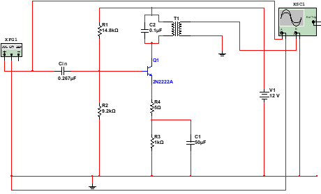
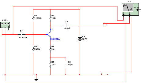
Figure 1 illustrates the circuit diagram of the conventional single-stage common-emitter transistor amplifier designed using a 2N2222A NPN bipolar junction transistor (BJT). The amplifier employs a voltage-divider bias network to establish a stable quiescent operating point, while the collector resistor provides broadband voltage amplification.
The input and output coupling capacitors isolate the DC biasing network while allowing the AC signal to pass through the amplifier stages and the emitter bypass capacitor enhances the AC voltage gain by reducing emitter degeneration. A 12 V DC supply and a 10 mV peak sinusoidal input signal were used throughout the simulation. This circuit served as the reference amplifier for the study. During the design of the single-stage tuned common-emitter amplifier, all design parameters, including the transistor type, supply voltage, bias network, quiescent operating point, and passive components, were retained. The only modification was the replacement of the collector resistor (RC) with a parallel LC resonant circuit. The resonant frequency of the tuned circuit was determined from :
f0=12πLC(17)
At resonance, the inductive and capacitive reactance are equal (XL=XC), causing the parallel LC circuit to exhibit maximum impedance. This high impedance effectively replaces the resistive collector load and enables selective amplification of signals near the resonant frequency.
Figure 1. Conventional single-stage common-emitter transistor amplifier.
2.3. Design of the Single-Stage Tuned Common-Emitter Transistor Amplifier.
Figure 2 illustrates the circuit diagram of the designed single-stage tuned common-emitter transistor amplifier developed using a 2N2222A NPN bipolar junction transistor (BJT). The circuit was developed under the same operating conditions as the conventional single-stage common-emitter amplifier to enable a fair comparative performance evaluation. The same 2N2222A NPN transistor, supply voltage (VCC), voltage-divider bias network (R1 and R2), emitter resistor (RE), input coupling capacitor (Cin), and emitter bypass capacitor (CE) were retained. The only modification was the replacement of the collector resistor with a parallel LC resonant circuit connected across the primary winding of a 1: 1 transformer, thereby making the amplifier frequency selective. The resonant frequency of the tuned circuit was selected as f0=1kHz Using a standard capacitor value of C = 0.1μF, the required inductance was determined from the resonance equation:
L=12πf02C(18)
Substituting, f0=1kHz and C = 0.1μF gives
L=12×3.142×10002(1×10⁻⁷)
L=1(6284)2×10⁻⁷
L=13.948×107×10-7
L=13.948
L = 0.253H
The resonant circuit parameters were therefore selected as follows:
1) Resonant frequency (f0)=1kHz,
2) Capacitor (C) = 0.1μF and
3) Inductor(L) = 0.253H
The transformer was modeled with a primary inductance of 0.253 H, a secondary inductance of 0.253 H, and a coupling coefficient of 0.99. At resonance, the parallel LC circuit presents a maximum impedance to the collector, thereby producing the largest voltage swing across the collector load and maximizing the amplifier voltage gain. Signals away from the resonant frequency encounter lower collector impedance and are therefore attenuated, providing the desired frequency selectivity. Unlike the conventional amplifier, no output coupling capacitor was used because the transformer provides electrical isolation between the collector circuit and the output, allowing only the amplified AC signal to be coupled through the secondary winding . Thus, the circuit shown in Figure 2 provides a narrow-band, frequency-selective amplifier suitable for comparing the voltage gain, resonant response, bandwidth, and frequency selectivity of the tuned amplifier with those of the conventional single-stage common-emitter transistor amplifier under identical operating conditions.
Figure 2. Single-stage tuned common-emitter transistor amplifier.
3. Simulation Procedure for Conventional and Tuned Common-Emitter Amplifiers
The peak voltage of each waveform was determined using Equation (17):
Vp=Number of Vertical Divisions×Channel Scale2(19)
where:
1) Vp= peak voltage (V)
2) Channel Scale = oscilloscope vertical scale (V/div or mV/div)
The voltage gain of each amplifier was calculated using Equation (Sobot 2013)(23):
Av=Vout(p)Vin(p)(20)
To facilitate comparison using the standard representation adopted in electronics literature, the voltage gain was converted to decibels (dB) using:
AV(dB)=20log10(AV)(21)
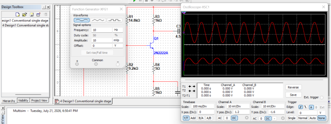
The conventional single-stage common-emitter transistor amplifier was first simulated at an input frequency of 10 Hz using a sinusoidal input signal with a peak amplitude of 10 mV. The input and output waveforms were displayed simultaneously on the oscilloscope, as shown in Figure 3. For the input signal, Channel A was set to 10 mV/div, and the waveform occupied approximately 2 vertical divisions from peak to trough. Applying Equation (17),
Vin(p)=2×10mV2=10mV
For the output signal, Channel B was set to 10 mV/div, and the output waveform occupied approximately 4.8 vertical divisions from peak to trough. Therefore,
Vout(p)=4.8×10mV2=24mV
Substituting these values into Equation (18),
AV=24mV10mV  =2.4
The corresponding voltage gain in decibels is
AV=20log10(2.4)=7.60dB
Therefore, the conventional single-stage common-emitter transistor amplifier produced a voltage gain of 2.4, corresponding to 7.60 dB at 10 Hz.
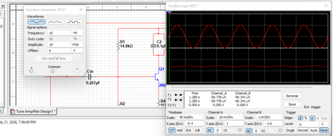
The same measurement procedure was repeated for all selected frequencies between 10 Hz and 100 MHz while maintaining the input signal at 10 mV peak. The measured output voltages were used to calculate the corresponding voltage gains, and the results are presented in Table 1. Similarly, the single-stage tuned common-emitter transistor amplifier was simulated under the same operating conditions using an input frequency of 10 Hz and a sinusoidal input signal with a peak amplitude of 10 mV. The corresponding input and output waveforms are shown in Figure 4. For the input signal, Channel A was set to 10 mV/div, and the waveform occupied approximately 2 vertical divisions. Hence,
Vin(p)=2×10mV2=10mV
For the output signal, Channel B was set to 1 mV/div, and the waveform occupied approximately 0.5 vertical divisions. Therefore,
Vout(p)=0.5×1mV2=0.25mV
Substituting these values into Equation (18),
AV=0.25mV10mV  = 0.025
The corresponding voltage gain expressed in decibels (dB) is
AV=20log100.025=-32.04dB
Thus, the single-stage tuned common-emitter transistor amplifier produced a voltage gain of 0.025, corresponding to −32.04 dB at 10 Hz. Figure 3 illustrates the input and output waveforms of the conventional single-stage common-emitter transistor amplifier, whereas Figure 4 presents the corresponding waveforms for the single-stage tuned common-emitter transistor amplifier. The above procedure was repeated for all selected frequencies between 10 Hz and 100 MHz under identical simulation conditions, and the calculated voltage gains were subsequently used to construct the frequency-response curves and Bode magnitude plots presented in the Results and Discussion section.
Figure 3. Conventional Single-Stage Common Emitter Transistor Amplifier Waveform.
Figure 4. Single-Stage Tuned Common-Emitter Transistor Amplifier Waveform.
Table 1 Simulation data for the comparative performance evaluation of the conventional single-stage common-emitter transistor amplifier and the single-stage tuned common-emitter transistor amplifier. A constant 10 mV peak sinusoidal input signal was applied throughout the simulations. The measured output voltages were used to calculate the corresponding voltage gains in linear scale and decibels (dB), providing the basis for comparing the frequency response, bandwidth, and frequency-selective characteristics of the two amplifier configurations.
Table 1. Simulation Data for the Comparative Performance Evaluation of the Conventional Single-Stage Common-Emitter Transistor Amplifier and the Single-Stage Tuned Common-Emitter Transistor Amplifier.

Frequency

Input Voltage (mVp)

Conventional Amplifier Output (mVP)

Voltage Gain (V/V)

Gain (dB)

Tuned Amplifier Output (mVP)

Voltage Gain (V/V)

Gain (dB)

10Hz

10

24

2.40

7.60

0.25

0.025

-32.04

15Hz

10

44

4.40

12.87

1.45

0.145

-16.77

100Hz

10

800

80.00

38.06

170

17.00

24.61

200Hz

10

1600

160.00

44.08

690

69.00

36.78

500Hz

10

3250

325.00

50.24

4000

400.00

52.04

1KHz

10

4000

400.00

52.04

40000

4000.00

72.04

10KHz

10

4700

470.00

53.44

2500

250.00

47.96

100KHz

10

5000

500.00

53.98

124

12.40

21.87

1MHz

10

5000

500.00

53.98

12.5

1.25

1.94

10MHz

10

4500

450.00

53.06

1.25

0.125

-18.06

20MHz

10

3750

375.00

51.48

0.95

0.095

-20.45

50MHz

10

2750

275.00

48.79

0.25

0.025

-32.04

100MHz

10

1500

150.00

43.52

0.1

0.010

-40.00

4. Results and Discussion
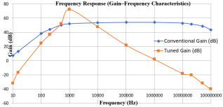
The frequency-response characteristics of the conventional and tuned single-stage common-emitter transistor amplifiers were evaluated using NI Multisim 11.0 over the frequency range of 10 Hz to 100 MHz The simulated voltage gains were converted to decibels (dB), and the corresponding Bode magnitude plot is presented in Figure 5, while the calculated values are summarized in Table 1. These results provide the basis for comparing the frequency response, bandwidth, and frequency-selective characteristics of the two amplifier configurations, thereby achieving the objectives of this study . Figure 5 shows that the conventional single-stage common-emitter transistor amplifier exhibits a broad and relatively flat mid-band frequency response. At low frequencies, the voltage gain is relatively small because the input coupling capacitor and emitter bypass capacitor introduce high reactance, which attenuates the input signal. As the frequency increases, the gain rises steadily from 7.60 dB at 10 Hz to approximately 54 dB over the mid-band region (100 kHz – 1 MHz), before gradually decreasing at higher frequencies because of the transistor's internal junction capacitances and other parasitic effects that limit high-frequency performance (Table 1; Figure 5). This behavior agrees with the theoretical frequency response of common-emitter transistor amplifiers reported by , confirming the wide bandwidth and stable mid-band performance of the conventional amplifier.
In contrast, the single-stage tuned common-emitter transistor amplifier exhibits a highly frequency-selective response. At low frequencies, the amplifier produces very low gain because the LC tuned circuit operates far below its resonant frequency and therefore does not efficiently transfer signal energy. As the input frequency approaches the designed resonant frequency of 1 kHz, the gain increases rapidly and reaches a maximum value of approximately 72.04 dB, after which it decreases sharply as the frequency moves away from resonance (Table 1; Figure 5). This behavior is consistent with the theory of tuned amplifiers, where maximum amplification occurs at resonance, the inductive and capacitive reactances are equal (XC=XL), causing the parallel LC circuit to present maximum impedance at the collector. Consequently, the voltage gain reaches its maximum value .
The comparison between the two amplifier configurations clearly demonstrates their different operating characteristics. Although the single-stage tuned common-emitter transistor amplifier provides significantly higher gain at its resonant frequency than the conventional amplifier, its useful operating bandwidth is much narrower because effective amplification occurs only within a limited frequency range around resonance. Conversely, the conventional single-stage common-emitter transistor amplifier provides a lower maximum gain but maintains relatively constant amplification over a much wider frequency range. Consequently, the conventional amplifier is more suitable for broadband amplification, whereas the tuned amplifier is better suited for narrow-band and frequency-selective applications such as radio-frequency receivers, communication circuits, and signal-selective amplification .
The Bode magnitude plot presented in Figure 5 further confirms these observations. The conventional amplifier exhibits a gradual increase in gain from 7.60 dB at 10 Hz to approximately 54 dB in the mid-band region before gradually rolling off at higher frequencies. In contrast, the tuned amplifier exhibits a pronounced resonant peak at approximately 1 kHz, followed by a rapid reduction in gain on both sides of the resonant frequency. These simulation results agree well with the theoretical characteristics of broadband and tuned transistor amplifiers reported in the literature .
Overall, the simulation results successfully fulfilled the objectives of this study by providing a comprehensive comparison of the frequency response, bandwidth, and frequency-selective characteristics of the conventional single-stage common-emitter transistor amplifier and the single-stage tuned common-emitter transistor amplifier. The conventional amplifier demonstrated excellent wideband performance with nearly constant mid-band gain, whereas the tuned amplifier produced substantially higher gain at its designed resonant frequency of 1 kHz but with a much narrower bandwidth. These findings are consistent with established transistor amplifier theory and demonstrate that the conventional amplifier is more suitable for broadband applications, while the tuned amplifier is preferred for selective frequency amplification .
Figure 5. Bode magnitude plot comparing the frequency response of the conventional single-stage common-emitter transistor amplifier and the single-stage tuned common-emitter transistor amplifier.
5. Conclusion
This study presented a comparative performance evaluation of a conventional single-stage common-emitter transistor amplifier and a single-stage tuned common-emitter transistor amplifier using NI Multisim 11.0 under identical operating conditions. The results showed that the conventional amplifier exhibited a broad frequency response with a relatively constant mid-band gain of approximately 54 dB, making it suitable for broadband signal amplification. In contrast, the tuned amplifier achieved a much higher peak gain of approximately 72.04 dB at its designed resonant frequency of 1 kHz, but its gain decreased rapidly outside the resonant frequency, resulting in a narrow bandwidth and excellent frequency selectivity. Therefore, the conventional amplifier is more appropriate for broadband applications, whereas the tuned amplifier is better suited for narrow-band and frequency-selective applications such as radio-frequency communication systems. Overall, the study fulfilled its objective by demonstrating the differences in voltage gain, frequency response, bandwidth, and frequency-selective characteristics of the two amplifier configurations. The findings provide useful guidance for the selection of suitable transistor amplifier configurations for broadband and narrow-band electronic and communication applications and may serve as a useful reference for future simulation-based amplifier design studies.
Abbreviations

AC

Alternating Current

BJT

Bipolar Junction Transistor

CE

Common-Emitter

DC

Direct Current

IF

Intermediate Frequency

LC

Inductor–Capacitor

NI

National Instruments

RF

Radio Frequency

AV

Voltage Gain

CE

Emitter Bypass Capacitor

Cin

Input Coupling Capacitor

Cout

Output Coupling Capacitor

IB

Base Current

IC

Collector Current

IE

Emitter Current

R1, R2

Voltage-Divider Bias Resistors

RC

Collector Resistor

RE

Emitter Resistor

Rg

Source Resistance

VB

Base Voltage

VBE

Base–Emitter Voltage

VCC

Supply Voltage

VCE

Collector–Emitter Voltage

VE

Emitter Voltage

XC

Capacitive Reactance

XL

Inductive Reactance

fo

Resonant Frequency

Author Contributions
Yusuf Abdullahi: Conceptualization, Data curation, Formal Analysis, Investigation, Methodology, Software, Visualization, Writing – original draft
Ismail Garba Saidu: Conceptualization, Methodology, Supervision, Validation, Writing – review & editing
Muhammad Bello Abdullahi: Formal Analysis, Methodology, Validation, Writing – review & editing
Kabir Ahmed Dabai: Investigation, Resources, Validation, Writing – review & editing
Buhari Bello Sahabi: Data curation, Validation, Writing – review & editing
Aisha Aminu Mode: Investigation, Validation, Writing – review & editing
Conflicts of Interest
The authors declare no conflicts of interest.
References
[1] Boylestad, R. L., & Nashelsky, L. (2019). Electronic Devices and Circuit Theory (12th ed.). Pearson.
[2] Cadiz, F., & Couairon, A. (2025). Electric Currents, Ohm’s Law and Electrical Networks. In Classical Electrodynamics: Fundamentals and Applications (pp. 215-266): Springer.
[3] Campos-Salazar, J. M., Aguayo-Lazcano, J. L., Rafiezadeh, R., & García-Rojas, G. (2025). Bipolar Junction Transistor Amplifiers—State-Space Modeling Across Frequencies. Journal of Electronics and Electrical Engineering.
[4] Casali, N., Cardani, L., Colantoni, I., Cruciani, A., Di Domizio, S., Martinez, M, Vignati, M. (2019). Phonon and light read out of a Li 2 MoO 4 crystal with multiplexed kinetic inductance detectors. The European Physical Journal C, 79(8), 724.
[5] Chen, C.-C. (2020). New method of finding exact frequency response for feedback amplifiers. IET Circuits, Devices & Systems, 14(7), 1048–1061.
[6] Christensen, D. A. (2022). Kirchhoff’s Voltage and Current Laws: Circuit Analysis. In Introduction to Biomedical Engineering: Biomechanics and Bioelectricity Part II (pp. 13-23): Springer.
[7] Clark, J. (2012). AC power conditioners: Design and application: Academic Press.
[8] Costa, L. d. F. (2018). Linearity Analysis of the Common Collector Amplifier, or Emitter Follower. arXiv preprint arXiv: 1805.02705.
[9] Floyd, T. L. (2021). Electronic Devices (11th ed.). Pearson.
[10] Gift, S. J., & Maundy, B. (2020). Bipolar Junction Transistor. In Electronic Circuit Design and Application (pp. 41-87): Springer.
[11] Horowitz, P., & Hill, W. (2015). The Art of Electronics (3rd ed.). Cambridge University Press.
[12] Leblebici, D., & Leblebici, Y. (2021). Frequency-Selective RF Circuits. In Fundamentals of High Frequency CMOS Analog Integrated Circuits (pp. 165-216): Springer.
[13] Litovski, V. (2023). 2 Biasing the Basic Electronic Amplifier Configurations. In Lecture Notes in Analogue Electronics: Electronic Signal Amplification and Linear Oscillators (pp. 5-39): Springer.
[14] Manocha, P., & Rincón-Mora, G. A. (2025). Transistor Frequency-Response Analysis: Recursive Shunt-Circuit Transformations. Electronics, 14(2), 296.
[15] Mercer, D., & Miclaus, A. (2020). ADALM2000 Activity: Frequency Response of a Common-Emitter BJT Amplifier. Analog Dialogue, 54(2).
[16] Moses, G. E., & Ebregbe, D. (2025). Design, Simulation and Performance Comparison of Four Single-Stage Amplifier Configurations. International Journal of Academic Engineering Research, 9(8), 166–179.
[17] National Instruments. (2010). NI Multisim User Guide. National Instruments.
[18] Noor, K. T., Islam, M. S., & Fuad, F. (2016). Analysis of power converters and smart power factor correction. BRAC University,
[19] Ruiz, D. (2010). Discrete time disturbance accommodation control of a buck-boost switching converter: University of Arkansas.
[20] Ryan, B. (2013). High Impedance Amplifiers for Non-Contact Bio-Potential Sensing. Open Access Te Herenga Waka-Victoria University of Wellington.
[21] Sapkota, M. (2026). Verification of Bias Circuit Design of Different Bipolar RF Transistors.
[22] Sedra, A. S., & Smith, K. C. (2021). Microelectronic Circuits (8th ed.). Oxford University Press.
[23] Self, D. (2013). Audio power amplifier design: Routledge.
[24] Sobot, R. (2013). RF and IF Amplifiers: Solutions. In Wireless Communication Electronics by Example (pp. 201-213): Springer.
[25] Strickland, J. R. (2016). Collector, Base, and Emitter. In Junk Box Arduino: Ten Projects in Upcycled Electronics (pp. 103-124): Springer.
[26] Van Rensburg, P. J., & Ferreira, H. C. (2003). Coupling circuitry: Understanding the functions of different components. Paper presented at the Proc. 7th Int. Symp. Power-Line Comm.
[27] Wang, R. (2025). Research on Performance Improvement of Common-Emitter Amplifiers Based on Bias Design Optimization. Paper presented at the 2025 7th International Conference on Electronic Engineering and Informatics (EEI).
[28] Wardhana, A. W., Ramadhani, Y., & Priswanto, P. (2022). Design and Simulation of a Multistages Common-Emitter, Common-Collector, AC Voltage Amplifier. Jurnal Nasional Teknik Elektro.
[29] Yusuf, A. i., Widada, W., & Taruno, W. P. (2022). Determine of the time constant of capacitance applied to electrical capacitance tomography. Paper presented at the 2022 International Conference on Informatics Electrical and Electronics (ICIEE).
Cite This Article
  • APA Style

    Abdullahi, Y., Saidu, I. G., Abdullahi, M. B., Dabai, K. A., Sahabi, B. B., et al. (2026). Comparative Performance Evaluation of Conventional and Tuned Single-Stage Common-Emitter Transistor Amplifiers Using Multisim 11.0. Journal of Electrical and Electronic Engineering, 14(5), 211-222. https://doi.org/10.11648/j.jeee.20261405.11

    Copy | Download

    ACS Style

    Abdullahi, Y.; Saidu, I. G.; Abdullahi, M. B.; Dabai, K. A.; Sahabi, B. B., et al. Comparative Performance Evaluation of Conventional and Tuned Single-Stage Common-Emitter Transistor Amplifiers Using Multisim 11.0. J. Electr. Electron. Eng. 2026, 14(5), 211-222. doi: 10.11648/j.jeee.20261405.11

    Copy | Download

    AMA Style

    Abdullahi Y, Saidu IG, Abdullahi MB, Dabai KA, Sahabi BB, et al. Comparative Performance Evaluation of Conventional and Tuned Single-Stage Common-Emitter Transistor Amplifiers Using Multisim 11.0. J Electr Electron Eng. 2026;14(5):211-222. doi: 10.11648/j.jeee.20261405.11

    Copy | Download

  • @article{10.11648/j.jeee.20261405.11,
      author = {Yusuf Abdullahi and Ismail Garba Saidu and Muhammad Bello Abdullahi and Kabir Ahmed Dabai and Buhari Bello Sahabi and Aisha Aminu Mode},
      title = {Comparative Performance Evaluation of Conventional and Tuned Single-Stage Common-Emitter Transistor Amplifiers Using Multisim 11.0},
      journal = {Journal of Electrical and Electronic Engineering},
      volume = {14},
      number = {5},
      pages = {211-222},
      doi = {10.11648/j.jeee.20261405.11},
      url = {https://doi.org/10.11648/j.jeee.20261405.11},
      eprint = {https://article.sciencepublishinggroup.com/pdf/10.11648.j.jeee.20261405.11},
      abstract = {The frequency response of transistor amplifiers is a key performance characteristic that determines their suitability for broadband and frequency-selective applications. This study comparatively evaluates the performance of a conventional single-stage common-emitter transistor amplifier and a tuned single-stage common-emitter transistor amplifier using NI Multisim 11.0. Both amplifier configurations were designed and simulated under identical operating conditions using a 2N2222A NPN transistor, a 12 V supply, identical biasing networks, and the same passive components. The only design difference was the replacement of the collector resistor in the conventional amplifier with a parallel LC resonant circuit in the tuned amplifier. The frequency response of both amplifiers was evaluated over the frequency range of 10 Hz to 100 MHz, and the voltage gains were calculated from the simulated output waveforms and expressed in decibels (dB). The results showed that the conventional amplifier maintained a nearly constant mid-band gain of approximately 54 dB over a wide frequency range, demonstrating excellent broadband performance. In contrast, the tuned amplifier produced a maximum gain of approximately 72.04 dB at its designed resonant frequency of 1 kHz, but exhibited a much narrower bandwidth due to its frequency-selective characteristics. The comparative analysis confirms that the conventional amplifier is better suited for broadband signal amplification, whereas the tuned amplifier is more appropriate for narrow-band and radio-frequency applications requiring high gain at a specific frequency. These findings provide useful guidance for selecting suitable transistor amplifier configurations for broadband and frequency-selective electronic and communication applications.},
     year = {2026}
    }
    

    Copy | Download

  • TY  - JOUR
    T1  - Comparative Performance Evaluation of Conventional and Tuned Single-Stage Common-Emitter Transistor Amplifiers Using Multisim 11.0
    AU  - Yusuf Abdullahi
    AU  - Ismail Garba Saidu
    AU  - Muhammad Bello Abdullahi
    AU  - Kabir Ahmed Dabai
    AU  - Buhari Bello Sahabi
    AU  - Aisha Aminu Mode
    Y1  - 2026/09/09
    PY  - 2026
    N1  - https://doi.org/10.11648/j.jeee.20261405.11
    DO  - 10.11648/j.jeee.20261405.11
    T2  - Journal of Electrical and Electronic Engineering
    JF  - Journal of Electrical and Electronic Engineering
    JO  - Journal of Electrical and Electronic Engineering
    SP  - 211
    EP  - 222
    PB  - Science Publishing Group
    SN  - 2329-1605
    UR  - https://doi.org/10.11648/j.jeee.20261405.11
    AB  - The frequency response of transistor amplifiers is a key performance characteristic that determines their suitability for broadband and frequency-selective applications. This study comparatively evaluates the performance of a conventional single-stage common-emitter transistor amplifier and a tuned single-stage common-emitter transistor amplifier using NI Multisim 11.0. Both amplifier configurations were designed and simulated under identical operating conditions using a 2N2222A NPN transistor, a 12 V supply, identical biasing networks, and the same passive components. The only design difference was the replacement of the collector resistor in the conventional amplifier with a parallel LC resonant circuit in the tuned amplifier. The frequency response of both amplifiers was evaluated over the frequency range of 10 Hz to 100 MHz, and the voltage gains were calculated from the simulated output waveforms and expressed in decibels (dB). The results showed that the conventional amplifier maintained a nearly constant mid-band gain of approximately 54 dB over a wide frequency range, demonstrating excellent broadband performance. In contrast, the tuned amplifier produced a maximum gain of approximately 72.04 dB at its designed resonant frequency of 1 kHz, but exhibited a much narrower bandwidth due to its frequency-selective characteristics. The comparative analysis confirms that the conventional amplifier is better suited for broadband signal amplification, whereas the tuned amplifier is more appropriate for narrow-band and radio-frequency applications requiring high gain at a specific frequency. These findings provide useful guidance for selecting suitable transistor amplifier configurations for broadband and frequency-selective electronic and communication applications.
    VL  - 14
    IS  - 5
    ER  - 

    Copy | Download

Author Information
  • Department of Applied Physics, Umaru Ali Shinkafi Polytechnic, Sokoto, Nigeria
  • Department of Physics, Usmanu Danfodiyo University, Sokoto, Nigeria

  • Department of Physics, Usmanu Danfodiyo University, Sokoto, Nigeria

  • Department of Electrical Engineering, Usmanu Danfodiyo University, Sokoto, Nigeria

  • Department of Applied Physics, Umaru Ali Shinkafi Polytechnic, Sokoto, Nigeria

  • Department of Microbiology, Usmanu Danfodiyo University, Sokoto, Nigeria