Research Article | | Peer-Reviewed

Optimization of Performance in Thin-Film CIGS Solar Cells: Silvaco Simulation of Doping and Absorber Layer Thickness

Received: 10 August 2025     Accepted: 19 August 2025     Published: 8 September 2025
Views:       Downloads:
Abstract

This study investigates the effects of doping concentration and absorber layer thickness on the performance of Cu(In,Ga)Se2 (CIGS) thin-film solar cells using detailed numerical simulations. The work focuses on identifying optimal design parameters to maximize power conversion efficiency by analyzing their influence on key device characteristics, including short-circuit current density, open-circuit voltage, and fill factor. The results indicate that the doping concentration critically impacts carrier transport and recombination dynamics. An optimal doping level of 6×1016 cm-3 enhances charge carrier collection, leading to simultaneous improvements in short-circuit current density, open-circuit voltage, and fill factor. Doping beyond this value increases series and shunt resistances, which reduces the efficiency gains, emphasizing the importance of precise doping control. The absorber layer thickness also plays a significant role in device performance. Increasing the thickness from 0.1 µm to 1 µm substantially improves photon absorption and carrier generation, resulting in a marked enhancement in efficiency. However, further increasing the thickness above 1 µm yields only marginal efficiency gains, as photon absorption reaches saturation and the recombination rate increases, highlighting the trade-off between absorption depth and minority carrier lifetime. Overall, the study demonstrates that careful optimization of both doping and absorber thickness is essential to achieving high-efficiency CIGS solar cells. Specifically, a doping concentration of 6×1016 cm-3 combined with an absorber thickness in the range of 0.1-1 µm provides the most favorable conditions for device performance. These findings offer practical guidelines for experimental fabrication and numerical optimization, contributing to the design of more efficient thin-film photovoltaic devices. The insights provided by this work can guide future research in enhancing the performance of CIGS solar cells and other related thin-film technologies.

Published in International Journal of Energy and Power Engineering (Volume 14, Issue 4)
DOI 10.11648/j.ijepe.20251404.11
Page(s) 96-106
Creative Commons

This is an Open Access article, distributed under the terms of the Creative Commons Attribution 4.0 International License (http://creativecommons.org/licenses/by/4.0/), which permits unrestricted use, distribution and reproduction in any medium or format, provided the original work is properly cited.

Copyright

Copyright © The Author(s), 2025. Published by Science Publishing Group

Keywords

CIGS Solar Cells, Doping, Absorber Thickness, Efficiency, Short-Circuit Current, Open-Circuit Voltage, Fill Factor

1. Introduction
CIGS is a material characterized by a direct optical bandgap, a high absorption coefficient in the visible range, and the ability to exhibit p-type conductivity without requiring external doping by impurities . However, the development of CIGS-based solar cells is limited by the availability and high cost of elements like indium and gallium , highlighting the need to optimize the performance of electronic devices based on this material. The objective of this study is to analyze the impact of doping rate and the reduction of the absorber layer thickness on the performance of thin-film CIGS solar cells. To achieve this, we conducted a numerical simulation of a model solar cell using the ATLAS software from SILVACO .
The study is structured in two main parts: the first part covers the state of the art of the structural, optical, and electrical properties of thin-film CIGS layers, while the second part presents the principle of the numerical simulation performed with ATLAS, the structure of the studied solar cell, the properties of materials and defects, and the analysis of the results obtained.
2. Properties of CIGS Thin Films
2.1. Structural Properties
Copper indium diselenide (CuInSe2), often referred to as CIS, crystallizes in the chalcopyrite phase, which is derived from the zinc blende structure of ZnS. The chalcopyrite structure of CIS is a tetragonal system composed of two face-centered cubic lattices that are stacked and offset by one-quarter of the diagonal. In this structure, each selenium (Se) atom is surrounded by two copper (Cu) atoms and two indium (In) atoms. Consequently, each cation (Cu+ or In3+) is surrounded by four selenium anions (Se4-) .
By convention, the smaller edge is denoted as 'a' and the larger edge as 'c'. These are known as lattice parameters, with values reported in the literature as: a = 5.782Å and c = 11.620Å. If the temperature exceeds 800°C, the anions move from their tetrahedral sites. In this case, the cations (Cu+ and In3+) randomly occupy cationic sites, forming tetrahedra whose centers are occupied by anions (Se4-). As a result, the CIS structure transitions from the chalcopyrite phase to the sphalerite phase . Both of these structures are illustrated in Figure 1 .
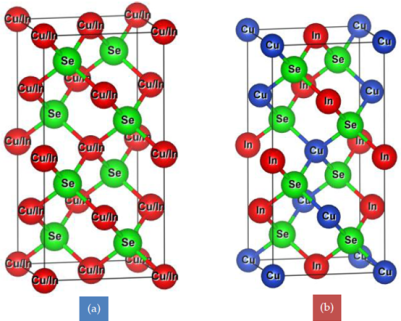
Figure 1. CIGS Structure (a): Sphalerite (b): Chalcopyrite.
Copper indium gallium diselenide (CuIn1-xGaxSe2), abbreviated as CIGS, also crystallizes in the chalcopyrite phase, similar to CIS, from which it is derived by partially substituting indium with gallium atoms. In the case of CIGS, the lattice parameters vary according to the gallium content, defined by X=Ga/(In+Ga), following the linear functions given by :
a=5.784-0.175x(1)
c=11.608-0.572x(2)
Thus, the structure of CIGS is influenced by the gallium content and is often determined using X-ray diffraction. This technique is based on the principle of Rayleigh scattering, which produces alternating constructive and destructive interference. When the interference is constructive, the interplanar spacing can be calculated using Bragg's law:
2dhkl.sinθ=n.λ (3)
where dhkl (cm) is the interplanar distance, θ (degrees) is the diffraction angle, n is the diffraction order, and λ (cm) is the wavelength of the X-ray beam.
The structure of CIGS is tetragonal (α = β = γ = π2 et a = b c), and the lattice parameters (a and c) can be determined using the following relation:
1dhkl=h2+ k2a2+l2c2 (4)
where h, k, and l are the Miller indices .
2.2. Optical Properties
CIGS is a direct bandgap semiconductor, with a high absorption coefficient in the visible and near-infrared range (105 cm⁻¹). It can be determined from the following relation:
α=1d ln(1-R)22T+ (1-R)42T2+ R2 (5)
where α (cm-1) is the absorption coefficient, d(µm) is the layer thickness, R is the reflection coefficient, and T is the transmission coefficient .
Other studies show that the optical bandgap of such a semiconductor is related to its absorption coefficient by the relation:
(αhν)²=A(-Eg)(6)
where A (J.cm-2) is a proportionality constant, (J.s) is Planck’s constant, ν(Hz) is the frequency, and Eg(eV) is the bandgap.
The optical bandgap of CIGS also depends on the gallium content, and it can be adjusted between 1.04 eV for CuInSe2 and 1.68 eV for CuGaSe2. In several studies, it has been approximated by the following relation:
Eg=1,04+0,64x-0.15x1-x(7)
For CIGS-based solar cells, the best efficiencies have been obtained with an optical bandgap of around 1.2 eV, corresponding to an X value of about 0.3. However, theoretical predictions indicate that the optimal bandgap for this material is 1.5 eV, which would allow it to absorb a wider range of wavelengths from the solar spectrum and thus improve efficiency .
The optical bandgap of CIGS can be determined using UV-Visible spectroscopy. By analyzing the transmittance spectrum of CIGS, the α2=f(hν) curve can be plotted to deduce its optical bandgap Eg or the width of its forbidden band .
2.3. Electrical Properties
CIS can exhibit either n-type or p-type conductivity without external doping. This internal doping is due to the presence of intrinsic defects that depend on the composition, technique, and growth conditions of the material. The concentration of these defects is given by Neumann's relation:
Ndeff=N0exp(-HfKT)(8)
where Hf (eV) is the formation enthalpy, K (J.s-1) is the Boltzmann constant, Ndeff (cm-3) is the defect concentration at temperature (K) and N0 is a constant.
Deviations from the molecular and stoichiometric balance of valence are given by the relations:
X = [Cu][In] -1(9)
Y = 2[Se]Cu+3[In] -1(10)
where [Cu], [In] and [Se] are the concentrations of Cu, In, and Se in CuInSe2 .
Neumann established, based on the values and signs of ΔX and ΔY, a correlation between the composition of CIS and its conductivity. For polycrystalline films with small deviations from the ideal stoichiometry, p-type conduction is always observed. However, for single-crystal films, n-type conduction is observed for ΔX>0 and ΔY<0, or ΔX<0 and ΔY<0 with small deviations from the ideal stoichiometry .
Unlike CIS, which can be either n-type or p-type, thin-film CIGS is always p-type. This could be explained by the reduction of the formation energy of deep defects, such as CuIn and VCu, in the presence of gallium .
The electrical properties of CIGS thin films can be determined using the Hall effect measurement technique. This method involves applying a magnetic field perpendicular to the layer, generating an electric voltage called the Hall voltage. By measuring this Hall voltage for precise current and magnetic field values, the concentration of carriers (electrons and holes) and their mobility can be determined .
3. Numerical Simulation
3.1. Principle
The principle of numerical simulation for semiconductor-based devices relies on solving a set of fundamental equations. These equations, derived from Maxwell's equations, mainly include the Poisson equation, the continuity equations, and the transport equations. During this process, a simulator such as the ATLAS software calculates, at every point in space and at each instant, the carrier concentrations (electrons and holes) in the device, as well as the electrostatic potential.
i) Poisson’s Equation
Poisson’s equation relates the variations in electrostatic potential to the volumetric charge density, and is expressed as:
V+ρε=0 (11)
where V is the electrostatic potential, ε is the dielectric permittivity, and ρ is the volumetric charge density.
ii) Continuity Equation
The continuity equations for electrons and holes are given by:
nt=+1qdivJn+Gn-Rn (12)
pt=-1qdivJp+Gp-Rp (13)
where, Jn and JP represent the current density of electrons and holes, Gn and Gp are the generation rates of electrons and holes, while Rn and Rp are the recombination rates of electrons and holes.
In the steady state, the carrier concentration no longer depends on time, and the continuity equations become:
-1qdivJn=Gn-Rn(14)
+ 1qdivJp=GP-RP(15)
iii) Transport Equations
The transport equations, derived by approximating current densities using a drift-diffusion model based on Boltzmann transport theory, are given by the following relations:
Jn=qnμnEn+qDnn (16)
Jp=qpμpEp+qDpp(17)
where Dn is the electron diffusion coefficient and Dp is the hole diffusion coefficient, given by the Einstein relations:
Dn=KTqμn (18)
Dp=KTqμp (19)
with, µn being the electron mobility, µp the hole mobility, K the Boltzmann constant, and q the elementary charge.
The above equations are taken from the user manual of the ATLAS - SILVACO modeling and simulation software .
3.2. Simulation Structure and Parameters
In this work, an experimental CIGS thin-film solar cell was modeled and simulated using the ATLAS - SILVACO software. The cell was fabricated by screen printing, and its structure is as follows: Pt-Al/ZnO/CdS/CIGS/Mo/PET .
To avoid shading effects that reduce illumination and thus efficiency, the Pt-Al grid was replaced by two aluminum contacts. Aluminum is a highly conductive, lightweight, and chemically stable metal, resistant to corrosion through the formation of a protective alumina (Al₂O₃) layer. This makes it a suitable material for photovoltaic applications such as CIGS thin-film solar cells .
The structure diagram is shown in Figure 2.
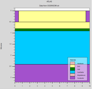
Figure 2. Schematic of the simulated structure.
The simulation parameters used in this study are derived from the literature, particularly from references .
We used the following models in our simulation:
The Shockley-Read-Hall (SRH) recombination model for defects. In this model, the recombination rate for a trap iii is given by:
RSRH,i= pn- ni2τn(p+niexpEi- EtKT)+ τp(n+niexpEt- EiKT)  (20)
where Ei  is the Fermi energy level in the intrinsic semiconductor, τn is the electron lifetime and τp is the hole lifetime. These lifetimes are given by the following relations:
τn=1σnvthNt (21)
τp=1σpvthNt (22)
where σn and σp are the capture cross sections for electrons and holes by a trap i, vth is the thermal velocity of carriers, and Nt is the trap density at an energy level Et.
The model for recombination at interface and contact states: this is the recombination at the defects present at the CdS/CIGS interface and at the front and back contacts. It is modeled by a fixed recombination rate of 105 m/s in our study.
The defect density model: the materials used in our study contain a large number of defects. These donor state defects for CIGS and acceptor state defects for CdS and ZnO are modeled by a Gaussian distribution given by:
gGAE=NGAexp-EGA-EWGA2 (23)
gGDE=NGDexp-E-EGDWGD2 (24)
where NGA and NGD are the acceptor and donor defect state densities, E is the defect energy, WGA and WGD are the standard deviations, and, EGA and EGD are the Gaussian peak energies .
Table 1. Material Properties.

Materials

CIGS

CdS

ZnO

Optical bandgap Eg300(eV)

1.2

2.4

3.3

Thickness d(µm)

1.5

0.1

0.8

Electron affinity χ(eV)

4.8

4.5

4.1

Relative dielectric permittivity εr

13.6

10

9

Effective electron state density NC300 (cm-3)

2.2. e18

2.2. e18

2.2. e18

Effective hole state density NV300 (cm-3)

1.8.e19

1.8.e19

1.8.e19

Electron mobility μn (cm².V-1.s-1)

100

100

100

Hole mobility μp (cm².V-1.s-1)

25

25

25

Electron lifetime τn(s)

1.e-7

1.e-7

1.e-7

Hole lifetime μp(s)

1.e-7

1.e-7

1.e-7

Acceptor concentration NA (cm-3)

2.e16

Donor concentration (cm-3)

1.e18

1.e18

Table 2. Defect Properties.

Materials

CIGS

CdS

ZnO

Gaussian defect

NDG=1.e14

NDA=1.e15

NDA=1.e15

Standard deviation WGA and WGD (eV)

0.1

0.1

0.1

Peak energy EGA and EGD (eV)

0.6

1.2

1.65

Electron capture cross section σn (cm2)

1.e-17

1.e-17

1.e-17

Hole capture cross section σp (cm²)

1.e-15

1.e-15

1.e-15

4. Results and Discussion
4.1. Effect of Doping Rate in the Absorber Layer
i) Effect of the doping rate of the absorber layeron the current-voltage characteristic
Figure 3 below shows the current density versus voltage characteristic for different doping values of the absorber layer.
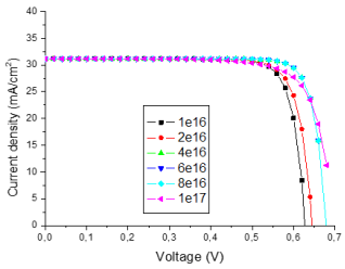
Figure 3. Current-voltage characteristic J(V) for different doping rates of the CIGS absorber layer.
Figure 3 shows the J(V) characteristics for different doping rates of the absorber layer. For NA= 4e16 and 6e16 cm-3 the characteristics are identical, as well as for NA= 8e16 and 1e17 cm-3. Aside from these two observations, we note that doping has almost no effect on the short-circuit current, but its influence is more pronounced on the open-circuit voltage, which increases with doping. To clarify these two effects further, we will next plot the current density and open-circuit voltage as a function of doping.
ii) Effect of the doping rate of the absorber layer on the current density
As mentioned in the previous paragraph, Figure 4 displays the short-circuit current density profile as a function of the doping rate of the absorber layer, in order to better observe its influence on the current density.
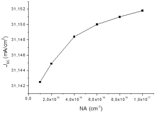
Figure 4. Short-circuit Current density as a function of the doping of the CIGS absorber layer.
Figure 4 shows that the current density increases from 31.1425 to 31.1518 mA/cm2 when the doping rate of the absorber layer changes from 1e16 to 1e17. Here, we observe a very slight increase in the short-circuit current density (JSC) with doping (+0,01 mA/cm² for a decade increase in doping). This can be explained by the behavior of the series resistance in the solar cell.
As the doping of the absorber layer increases, the carrier concentration in the material also increases, which could theoretically increase the photogenerated current, and therefore the short-circuit current density (JSC). However, a higher doping concentration also leads to an increase in the series resistance of the cell, which is related to the material and contact resistance.
The series resistance, which is inversely proportional to the material's conductivity, is influenced by carrier mobility. At higher doping concentrations, although the carrier density increases, the carrier mobility tends to decrease due to increased collisions with defects and traps. This means that the material's conductivity may not increase proportionally with doping, and could even decrease, especially if additional defects are introduced.
Thus, the series resistance becomes more significant as the doping concentration increases, limiting the increase in JSC. A high series resistance reduces the efficiency of carrier transport through the cell, preventing a significant increase in JSC., despite a higher doping level .
In summary, the marginal increase in JSC with increasing doping can be explained by the impact of series resistance, which, as it increases, limits current generation despite the increase in carrier density. This phenomenon emphasizes the importance of finding an optimal balance between doping, carrier mobility, and series resistance to maximize solar cell efficiency.
iii) Effect of the doping rate of the absorber layer on the open-circuit voltage
Figure 5 displays the open-circuit voltage profile as a function of the doping rate of the absorber layer.
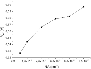
Figure 5. Open-circuit voltage as a function of the doping of the CIGS absorber layer.
Figure 5 shows that the open-circuit voltage increases from 0.6270 to 0.6970 V as the doping rate of the absorber layer increases from 1e16 to 1e17. In the same context, the open-circuit voltage (VOC) increases by 0.07 V for a tenfold increase in the doping concentration of the absorber layer. This phenomenon can be explained by the combined effects of series resistance and the reduction in recombination with increasing doping.
The increase in open-circuit voltage with doping can mainly be attributed to a reduction in recombination losses, as well as to better carrier separation. However, this effect is counterbalanced by series resistance, although it has less impact on VOC than on JSC. Therefore, doping improves the cell's performance by increasing VOC, but this must be balanced with the management of series resistance to optimize overall efficiency.
In addition to the series resistance, the shunt resistance plays an important role in the overall performance of the solar cell, especially in its effect on the open-circuit voltage (VOC). The shunt resistance has a significant effect on the open-circuit voltage, particularly when it is low, as it causes current to bypass the active region of the solar cell, leading to energy losses and a reduction in VOC. While doping can improve the open-circuit voltage by reducing recombination losses, it can also lead to a decrease in shunt resistance if it introduces defects. Therefore, optimizing both the doping concentration and the material quality to minimize shunt resistance is crucial for improving the overall efficiency of the solar cell .
In summary, shunt resistance and dopant concentration must be carefully managed to balance the effects on recombination and leakage currents, which ultimately determines the performance of the solar cell.
iv) Effect of the doping rate of the absorber layer on the fill factor
Figure 6 shows the profile of the fill factor as a function of the doping of the absorber layer.
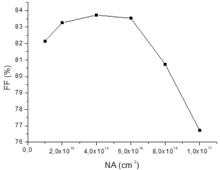
Figure 6. Fill factor as a function of the doping of the CIGS absorber layer.
Figure 6 shows that the fill factor (FF) increases from 82.1497 to 83.5307% as the doping rate of the absorber layer increases from 1e16 to 6e10 cm-3. his increase in the fill factor is mainly due to an improvement in carrier separation and a reduction in recombination losses, as indicated by the results observed for short-circuit current density (JSC) and open-circuit voltage (VOC). As doping increases, the carrier concentration in the absorber layer also increases, which theoretically enhances the photogenerated current, thus improving JSC and increasing the fill factor. Moreover, the reduction of recombination losses and the improvement in carrier separation contribute to a positive effect on the fill factor, which is a key indicator of the overall efficiency of the cell.
However, the fill factor decreases from 83.5307 to 76.7180% as the current density increases from 6e16 to 1e17 cm-3, despite the increase in doping. This phenomenon is mainly linked to the increase in series resistance and shunt resistance. As doping concentration continues to rise, additional defects may be introduced into the material, which increases the shunt resistance, thereby reducing the efficiency of the cell. The increase in series resistance is also a limiting factor, as it reduces the efficiency of carrier transport through the cell, which can lower the overall performance, even if the current density increases.
In summary, while increasing doping improves carrier generation and increases the fill factor up to a certain point, excessive doping can introduce additional defects into the material, increasing both series and shunt resistances. This limits the positive impact of doping on performance, highlighting the importance of finding an optimal balance between carrier density, carrier mobility, and the resistances of the cell to maximize the fill factor and overall efficiency of the solar cell.
v) Effect of the doping rate of the absorber layer on the efficiency
Figure 7 shows the profile of the efficiency as a function of the doping of the absorber layer.
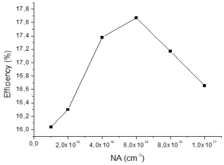
Figure 7. Efficiency as a function of the doping of the CIGS absorber layer.
Figure 7 shows that the efficiency increases from 16.04 to 17.67% as the doping rate of the absorber layer increases from 1e16 to 6e16 cm-3. However, the efficiency decreases from 17.67% to 16,66% when the doping rate of the absorber layer increases from 6e16 to 1e17 cm-3. This indicates that the optimal doping rate for the absorber layer is 6e16 cm-3, which is consistent with existing theories on doping optimization for CIGS cells .
In conclusion, the doping rate of the absorber layer significantly affects the performance of CIGS-based solar cells. The maximum efficiency of 17.67% is achieved with a doping rate of 6e16 cm-3, as demonstrated in this study. This observation confirms the existence of an optimal doping level, beyond which further doping increases can lead to a decrease in efficiency due to increased recombination and higher series resistance.
In this first part, we studied the effect of the doping rate of the absorber layer on the performance of CIGS-based solar cells. The results show that doping has a significant impact on several key parameters, including short-circuit current density (JSC), open-circuit voltage (VOC), and fill factor (FF). We observed an increase in efficiency from 16.04% to 17.67% when the doping rate of the absorber layer increased from 1e16 cm-3 to 6e16 cm-3, with a slight decrease in efficiency when the doping rate reached 1e17 cm-3. This behavior confirms that the optimal doping level for maximizing cell performance is 6e16 cm-3, which aligns with existing theory.
The results highlight that, although increasing doping improves carrier generation and reduces recombination losses, excessively high doping can introduce additional defects, increasing both series and shunt resistances, thereby limiting performance gains.
In the next part of this study, we will examine the influence of the absorber layer thickness on the cell’s performance, using the optimal doping rate found in this section, 6e16 cm-3. This analysis will allow us to determine how the thickness of the layer, in interaction with the optimal doping rate, can further affect the overall performance of the solar cell.
4.2. Effect of the Thickness of the CIGS Absorber Layer on the Performance of the Cells
i) Effect of the thickness of the absorber layer on the current-voltage characteristic
Figure 8 below shows the current density versus voltage characteristic for different thickness of the CIGS absorber layer.
Figure 8 shows that the J(V) characteristics are almost identical when the absorber layer thickness ranges from 0.3 to 3 µm. A slight shift in the curve is observed near the open-circuit voltage for an absorber layer thickness of 0.1 µm. To further analyze the influence of the absorber layer thickness, the profiles of short-circuit current density, open-circuit voltage, fill factor, and efficiency will be plotted in the following sections as a function of this layer thickness.
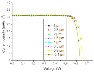
Figure 8. Current-voltage characteristic J(V) for different thickness of the CIGS absorber layer.
ii) Effect of the absorber layer thickness on the Short-circuit current density
Figure 9 displays the short-circuit current density profile as a function of the thickness of the absorber layer.
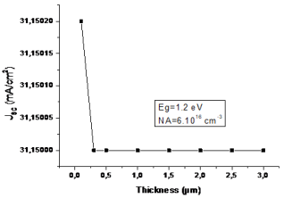
Figure 9. Short-circuit Current density as a function of the thickness of the CIGS absorber layer.
The short-circuit current density shows a slight decrease as the absorber layer thickness increases from 100 nm to 300 nm, which can be attributed to a reduction in the efficiency of carrier diffusion in the layer. However, beyond 300 nm, the current density remains constant up to 3 µm, suggesting that photon absorption reaches a saturation point, where further increases in layer thickness no longer significantly improve carrier generation. This behavior aligns with observations in the literature, where optimal absorber layer thicknesses exist, beyond which performance no longer increases.
iii) Effect of the absorber layer thickness on the open-circuit voltage
Figure 10 displays the open-circuit voltage profile as a function of the thickness of the absorber layer.
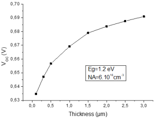
Figure 10. Open-circuit voltage as a function of the thickness of the CIGS absorber layer.
Figure 10 shows that as the absorber layer thickness decreases from 3 µm to 0.1 µm, the open-circuit voltage slightly decreases from 0.6910 V to 0.6348 V. This decrease in VOC with the reduced absorber layer thickness, particularly below 0.3 µm, is mainly due to the reduction in the minority carrier diffusion length, which increases recombination and limits carrier generation. On the other hand, when the layer thickness increases from 0.1 µm to 3 µm, carrier generation increases due to improved photon absorption, leading to an increase in open-circuit voltage. This evolution highlights the trade-off between photon absorption and carrier recombination in absorber layers of different thicknesses.
iv) Effect of the absorber layer thickness on the fill factor
Figure 11 displays the fill factor profile as a function of the thickness of the absorber layer.
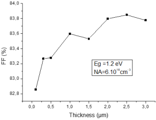
Figure 11. Fill factor as a function of the thickness of the CIGS absorber layer.
Figure 11 shows that as the absorber layer thickness increases from 0.5 µm to 3 µm, the fill factor (FF) increases slightly, from 83.2667% to 83.7763%. However, this increase is more significant when the absorber layer thickness changes from 0.1 µm to 0.5 µm. This trend can be explained by several factors related to the optimization of photon absorption and the reduction of recombination losses.
This analysis shows that increasing the absorber layer thickness improves the fill factor up to a certain thickness, after which the gains become marginal. The 0.1 to 0.5 µm range is therefore particularly optimal for maximizing carrier generation and reducing recombination losses, leading to a significant improvement in cell efficiency.
v) Effect of the absorber layer thickness on the efficiency
Figure 12 displays the efficiency profile as a function of the thickness of the absorber layer.
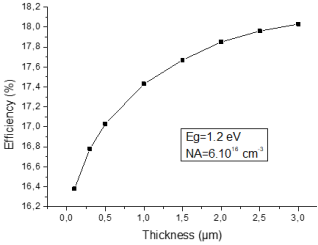
Figure 12. Efficiency as a function of the thickness of the CIGS absorber layer.
Figure 12 shows that when the absorber layer thickness increases from 1 µm to 3 µm, the efficiency increases slightly from 17.03% to 18.03%. However, when the absorber layer thickness increases from 0.1 µm to 1 µm, the increase in efficiency is more significant.
The increase in efficiency is more significant when the absorber layer thickness increases from 0.1 µm to 1 µm, as this optimizes photon absorption. Beyond 1 µm, absorption reaches a saturation point, and increasing the thickness has a more limited impact on efficiency.
In conclusion, while increasing the absorber layer thickness beyond 1 µm may have a limited effect on carrier generation, a thickness between 0.1 µm and 1 µm appears optimal for maximizing efficiency. This analysis provides valuable insights into the trade-off between carrier generation and recombination losses, paving the way for optimizing the layer thickness to enhance the overall performance of the solar cell.
5. Conclusion
This study analyzed the impact of doping and absorber layer thickness on the performance of CIGS solar cells. The optimal doping of 6e16 cm-3 improves short-circuit current density, open-circuit voltage, and fill factor, but higher concentrations increase shunt and series resistance, limiting gains.
Regarding the absorber layer thickness, a thickness between 0.1 µm and 1 µm maximizes photon absorption and carrier generation, thereby increasing efficiency. Beyond 1 µm, absorption reaches saturation, limiting further efficiency improvements.
In summary, optimal management of doping and absorber layer thickness is essential to maximize the efficiency of CIGS solar cells. The results of this study provide a solid foundation for the design and optimization of these cells.
Abbreviations

ATLAS

Advanced Technology for Large Area Simulation (logiciel de simulation TCAD de SILVACO)

CdS

Cadmium Sulfide

CIGS

Copper Indium Gallium Selenide

CIS

Copper Indium Selenide

FF

Fill Factor

J(V)

Current-Voltage Characteristic

JSC

Short-Circuit Current Density

Mo

Molybdenum

NA

Acceptor Concentration

NC

Effective Density of States in the Conduction Band

NV

Effective Density of States in the Valence Band

PET

Polyethylene Terephthalate (Plastic Substrate)

Pt-Al

Platinum-Aluminum (Metal Grid/Contact)

RSH

Shunt Resistance

RS

Series Resistance

Se

Selenium

SRH

Shockley-Read-Hall (Recombination Model)

VOC

Open-Circuit Voltage

ZnO

Zinc Oxide

Author Contributions
Alioune Ngom: Conceptualization, Data curation, Formal Analysis, Investigation, Methodology, Software, Validation, Writing - review & editing
Youssou Gning: Conceptualization, Data curation, Formal Analysis, Investigation, Methodology, Software, Supervision, Validation, Visualization, Writing - original draft, Writing - review & editing
Mamadou Lamine Samb: Conceptualization, Data curation, Formal Analysis, Investigation, Methodology, Resources, Software, Supervision, Validation, Visualization Writing - original draft, Writing - review & editing
Aly Toure: Conceptualization, Data curation, Formal Analysis, Investigation, Methodology, Software, Validation, Writing - review & editing
Moussa Toure: Conceptualization, Data curation, Formal Analysis, Investigation, Methodology, Project administration, Software, Supervision, Validation, Visualization, Writing - original draft, Writing - review & editing
Fatma Sow: Conceptualization, Formal Analysis, Investigation, Methodology, Software, Validation, Writing - review & editing
Mouhamadou Sam: Conceptualization, Formal Analysis, Investigation, Methodology, Software, Validation, Writing - review & editing
Ahmed Mohamed-Yahya: Conceptualization, Data curation, Formal Analysis, Funding acquisition, Investigation, Methodology, Project administration, Resources, Software, Supervision, Validation, Visualization, Writing - original draft, Writing - review & editing
Conflicts of Interest
The authors declare no conflicts of interest.
References
[1] S.-U. Park, R. Sharma, K. Ashok, S. Kang, J.-K. Sim, and C.-R. Lee, "A study on composition, structure and optical properties of copper-poor CIGS thin film deposited by sequential sputtering of CuGa/In and In/(CuGa+In) precursors," Journal of Crystal Growth, vol. 359, pp. 1-10, Nov. 2012,
[2] T. D. Lee and A. U. Ebong, "A review of thin film solar cell technologies and challenges," Renewable and Sustainable Energy Reviews, vol. 70, pp. 1286-1297, Apr. 2017,
[3] M. G. Faraj, K. Ibrahim, and A. Salhin, "Fabrication and characterization of thin-film Cu(In, Ga)Se2 solar cells on a PET plastic substrate using screen printing," Materials Science in Semiconductor Processing, vol. 15, no. 2, pp. 165-173, Apr. 2012,
[4] S. R. Kodigala, "Structural Properties of I-III-VI2 Absorbers," in Thin Films and Nanostructures, vol. 35, Elsevier, 2010, pp. 115-194.
[5] T. Unold and C. A. Kaufmann, "Chalcopyrite Thin-Film Materials and Solar Cells," in Comprehensive Renewable Energy, Elsevier, 2012, pp. 399-422.
[6] H. Yassine, "Synthèse et Caractérisation de Couches Minces de Cu(In,Ga)Se2 par Voie Electrochimique," Working Paper, Jan. 2021. Accessed: Jun. 20, 2024. Available:
[7] H. Joachim Möller, "Semiconductors for solar cell applications," Progress in Materials Science, vol. 35, no. 3-4, pp. 205-418, Jan. 1991,
[8] D. Alderton, "X-Ray Diffraction (XRD)," in Encyclopedia of Geology, Elsevier, 2021, pp. 520-531.
[9] S. R. Kodigala, "Optical Properties of I-III-VI2 Compounds," in Thin Films and Nanostructures, vol. 35, Elsevier, 2010, pp. 195-317.
[10] T. Ghorbani, M. Zahedifar, M. Moradi, and E. Ghanbari, "Influence of affinity, band gap and ambient temperature on the efficiency of CIGS solar cells," Optik, vol. 223, p. 165541, Dec. 2020,
[11] V. Foidart, "Étude des propriétés opto-électroniques de cellules solaires composées d’alliages de type kësterite en films minces," Université de Liège, 2019. Available:
[12] H. Neumann, N. Van Nam, H.-J. Höbler, and G. Kühn, "Electrical properties of n-type CuInSe2 single crystals," Solid State Communications, vol. 25, no. 11, pp. 899-902, Mar. 1978,
[13] C. Rincón and R. Márquez, "Defect physics of the CuInSe2 chalcopyrite semiconductor," Journal of Physics and Chemistry of Solids, vol. 60, no. 11, pp. 1865-1873, Nov. 1999,
[14] A. Rockett, "The Electronic effects of point defects in Cu(In x Ga 1−x)Se2," Thin Solid Films, vol. 361-362, pp. 330-337, Feb. 2000,
[15] W. Götz, R. S. Kern, C. H. Chen, H. Liu, D. A. Steigerwald, and R. M. Fletcher, "Hall-effect characterization of III-V nitride semiconductors for high efficiency light emitting diodes," Materials Science and Engineering: B, vol. 59, no. 1-3, pp. 211-217, May 1999,
[16] “ATLAS User’s Manual DEVICE SIMULATION SOFTWARE.” Copyright 2010.
[17] “Aluminium,” Wikipédia. May 16, 2025. Accessed: Aug. 06, 2025. Available:
[18] B. Bouanani, A. Joti, F. S. Bachir Bouiadjra, and A. Kadid, "Band gap and thickness optimization for improvement of CIGS/CIGS tandem solar cells using Silvaco software," Optik, vol. 204, p. 164217, Feb. 2020,
[19] [Sze, S. M.], & Ng, K. K. (2006). Physics of Semiconductor Devices. Wiley-Interscience.
[20] Aberle, A. G. (2001). Overview on SiN surface passivation of crystalline silicon solar cells. Solar Energy Materials and Solar Cells, 65(1-4), 239-248.
[21] C. Sajeev, N. Abraham, and K. L. Sreevidhya, "Defect states and grading induced bandgap variability analysis of CIGS solar cells through device simulations," Materials Today: Proceedings, vol. 43, pp. 3729-3734, Jan. 2021,
[22] K. Decock, S. Khelifi, and M. Burgelman, "Modelling multivalent defects in thin film solar cells," Thin Solid Films, vol. 519, no. 21, pp. 7481-7484, Aug. 2011,
Cite This Article
  • APA Style

    Ngom, A., Gning, Y., Samb, M. L., Toure, A., Toure, M., et al. (2025). Optimization of Performance in Thin-Film CIGS Solar Cells: Silvaco Simulation of Doping and Absorber Layer Thickness. International Journal of Energy and Power Engineering, 14(4), 96-106. https://doi.org/10.11648/j.ijepe.20251404.11

    Copy | Download

    ACS Style

    Ngom, A.; Gning, Y.; Samb, M. L.; Toure, A.; Toure, M., et al. Optimization of Performance in Thin-Film CIGS Solar Cells: Silvaco Simulation of Doping and Absorber Layer Thickness. Int. J. Energy Power Eng. 2025, 14(4), 96-106. doi: 10.11648/j.ijepe.20251404.11

    Copy | Download

    AMA Style

    Ngom A, Gning Y, Samb ML, Toure A, Toure M, et al. Optimization of Performance in Thin-Film CIGS Solar Cells: Silvaco Simulation of Doping and Absorber Layer Thickness. Int J Energy Power Eng. 2025;14(4):96-106. doi: 10.11648/j.ijepe.20251404.11

    Copy | Download

  • @article{10.11648/j.ijepe.20251404.11,
      author = {Alioune Ngom and Youssou Gning and Mamadou Lamine Samb and Aly Toure and Moussa Toure and Fatma Sow and Mouhamadou Sam and Ahmed Mohamed-Yahya},
      title = {Optimization of Performance in Thin-Film CIGS Solar Cells: Silvaco Simulation of Doping and Absorber Layer Thickness
    },
      journal = {International Journal of Energy and Power Engineering},
      volume = {14},
      number = {4},
      pages = {96-106},
      doi = {10.11648/j.ijepe.20251404.11},
      url = {https://doi.org/10.11648/j.ijepe.20251404.11},
      eprint = {https://article.sciencepublishinggroup.com/pdf/10.11648.j.ijepe.20251404.11},
      abstract = {This study investigates the effects of doping concentration and absorber layer thickness on the performance of Cu(In,Ga)Se2 (CIGS) thin-film solar cells using detailed numerical simulations. The work focuses on identifying optimal design parameters to maximize power conversion efficiency by analyzing their influence on key device characteristics, including short-circuit current density, open-circuit voltage, and fill factor. The results indicate that the doping concentration critically impacts carrier transport and recombination dynamics. An optimal doping level of 6×1016 cm-3 enhances charge carrier collection, leading to simultaneous improvements in short-circuit current density, open-circuit voltage, and fill factor. Doping beyond this value increases series and shunt resistances, which reduces the efficiency gains, emphasizing the importance of precise doping control. The absorber layer thickness also plays a significant role in device performance. Increasing the thickness from 0.1 µm to 1 µm substantially improves photon absorption and carrier generation, resulting in a marked enhancement in efficiency. However, further increasing the thickness above 1 µm yields only marginal efficiency gains, as photon absorption reaches saturation and the recombination rate increases, highlighting the trade-off between absorption depth and minority carrier lifetime. Overall, the study demonstrates that careful optimization of both doping and absorber thickness is essential to achieving high-efficiency CIGS solar cells. Specifically, a doping concentration of 6×1016 cm-3 combined with an absorber thickness in the range of 0.1-1 µm provides the most favorable conditions for device performance. These findings offer practical guidelines for experimental fabrication and numerical optimization, contributing to the design of more efficient thin-film photovoltaic devices. The insights provided by this work can guide future research in enhancing the performance of CIGS solar cells and other related thin-film technologies.
    },
     year = {2025}
    }
    

    Copy | Download

  • TY  - JOUR
    T1  - Optimization of Performance in Thin-Film CIGS Solar Cells: Silvaco Simulation of Doping and Absorber Layer Thickness
    
    AU  - Alioune Ngom
    AU  - Youssou Gning
    AU  - Mamadou Lamine Samb
    AU  - Aly Toure
    AU  - Moussa Toure
    AU  - Fatma Sow
    AU  - Mouhamadou Sam
    AU  - Ahmed Mohamed-Yahya
    Y1  - 2025/09/08
    PY  - 2025
    N1  - https://doi.org/10.11648/j.ijepe.20251404.11
    DO  - 10.11648/j.ijepe.20251404.11
    T2  - International Journal of Energy and Power Engineering
    JF  - International Journal of Energy and Power Engineering
    JO  - International Journal of Energy and Power Engineering
    SP  - 96
    EP  - 106
    PB  - Science Publishing Group
    SN  - 2326-960X
    UR  - https://doi.org/10.11648/j.ijepe.20251404.11
    AB  - This study investigates the effects of doping concentration and absorber layer thickness on the performance of Cu(In,Ga)Se2 (CIGS) thin-film solar cells using detailed numerical simulations. The work focuses on identifying optimal design parameters to maximize power conversion efficiency by analyzing their influence on key device characteristics, including short-circuit current density, open-circuit voltage, and fill factor. The results indicate that the doping concentration critically impacts carrier transport and recombination dynamics. An optimal doping level of 6×1016 cm-3 enhances charge carrier collection, leading to simultaneous improvements in short-circuit current density, open-circuit voltage, and fill factor. Doping beyond this value increases series and shunt resistances, which reduces the efficiency gains, emphasizing the importance of precise doping control. The absorber layer thickness also plays a significant role in device performance. Increasing the thickness from 0.1 µm to 1 µm substantially improves photon absorption and carrier generation, resulting in a marked enhancement in efficiency. However, further increasing the thickness above 1 µm yields only marginal efficiency gains, as photon absorption reaches saturation and the recombination rate increases, highlighting the trade-off between absorption depth and minority carrier lifetime. Overall, the study demonstrates that careful optimization of both doping and absorber thickness is essential to achieving high-efficiency CIGS solar cells. Specifically, a doping concentration of 6×1016 cm-3 combined with an absorber thickness in the range of 0.1-1 µm provides the most favorable conditions for device performance. These findings offer practical guidelines for experimental fabrication and numerical optimization, contributing to the design of more efficient thin-film photovoltaic devices. The insights provided by this work can guide future research in enhancing the performance of CIGS solar cells and other related thin-film technologies.
    
    VL  - 14
    IS  - 4
    ER  - 

    Copy | Download

Author Information